- 您現(xiàn)在的位置:買賣IC網(wǎng) > PDF目錄199476 > TS87C51RD2-VCLD 8-BIT MICROCONTROLLER PDF資料下載
參數(shù)資料
| 型號: | TS87C51RD2-VCLD |
| 元件分類: | 8位微控制器 |
| 英文描述: | 8-BIT MICROCONTROLLER |
| 中文描述: | 8位微控制器 |
| 文件頁數(shù): | 55/74頁 |
| 文件大?。?/td> | 689K |
| 代理商: | TS87C51RD2-VCLD |
第1頁第2頁第3頁第4頁第5頁第6頁第7頁第8頁第9頁第10頁第11頁第12頁第13頁第14頁第15頁第16頁第17頁第18頁第19頁第20頁第21頁第22頁第23頁第24頁第25頁第26頁第27頁第28頁第29頁第30頁第31頁第32頁第33頁第34頁第35頁第36頁第37頁第38頁第39頁第40頁第41頁第42頁第43頁第44頁第45頁第46頁第47頁第48頁第49頁第50頁第51頁第52頁第53頁第54頁當前第55頁第56頁第57頁第58頁第59頁第60頁第61頁第62頁第63頁第64頁第65頁第66頁第67頁第68頁第69頁第70頁第71頁第72頁第73頁第74頁
Rev. C - 06 March, 2001
59
TS80C51RA2/RD2
TS83C51RB2/RC2/RD2
TS87C51RB2/RC2/RD2
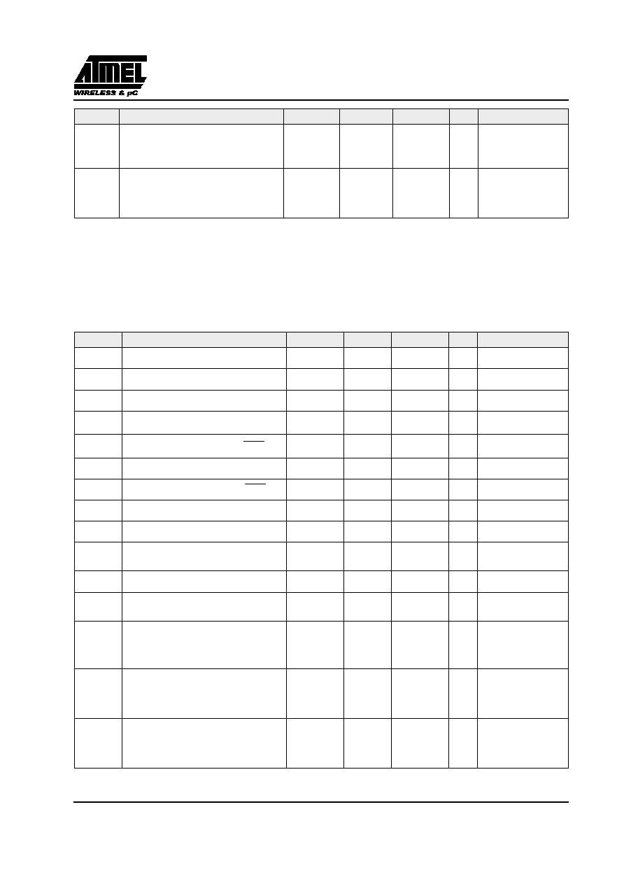
10.4. DC Parameters for Low Voltage
TA =0
°Cto+70°C; V
SS =0V;VCC = 2.7 V to 5.5 V ± 10%;F=0to30 MHz.
TA = -40
°Cto+85°C; V
SS =0V;VCC = 2.7 V to 5.5 V ± 10%;F=0to30 MHz.
Table 33. DC Parameters for Low Voltage
ICC
operating
Power Supply Current Maximum values, X1
mode: (7)
3 + 0.6 Freq
(MHz)
@12MHz 10.2
@16MHz 12.6
mA
VCC = 5.5 V
(8)
ICC
idle
Power Supply Current Maximum values, X1
mode: (7)
0.25+0.3Freq
(MHz)
@12MHz 3.9
@16MHz 5.1
mA
VCC = 5.5 V
(2)
Symbol
Parameter
Min
Typ
Max
Unit
Test Conditions
VIL
Input Low Voltage
-0.5
0.2 VCC - 0.1
V
VIH
Input High Voltage except XTAL1, RST
0.2 VCC + 0.9
VCC + 0.5
V
VIH1
Input High Voltage, XTAL1, RST
0.7 VCC
VCC + 0.5
V
VOL
Output Low Voltage, ports 1, 2, 3, 4, 5 (6)
0.45
V
IOL = 0.8 mA
(4)
VOL1
Output Low Voltage, port 0, ALE, PSEN (6)
0.45
V
IOL = 1.6 mA
(4)
VOH
Output High Voltage, ports 1, 2, 3, 4, 5
0.9 VCC
V
IOH = -10 A
VOH1
Output High Voltage, port 0, ALE, PSEN
0.9 VCC
V
IOH = -40 A
IIL
Logical 0 Input Current ports 1, 2, 3, 4, 5
-50
A
Vin = 0.45 V
ILI
Input Leakage Current
±10
A
0.45 V < Vin < VCC
ITL
Logical 1 to 0 Transition Current, ports 1, 2, 3,
4, 5
-650
A
Vin = 2.0 V
RRST
RST Pulldown Resistor
50
90 (5)
200
k
CIO
Capacitance of I/O Buffer
10
pF
Fc = 1 MHz
TA = 25
°C
IPD
Power Down Current
20 (5)
10 (5)
50
30
A
VCC = 2.0 V to 5.5 V
(3)
VCC = 2.0 V to 3.3 V
(3)
ICC
under
RESET
Power Supply Current Maximum values, X1
mode: (7)
1 + 0.2 Freq
(MHz)
@12MHz 3.4
@16MHz 4.2
mA
VCC = 3.3 V
(1)
ICC
operating
Power Supply Current Maximum values, X1
mode: (7)
1 + 0.3 Freq
(MHz)
@12MHz 4.6
@16MHz 5.8
mA
VCC = 3.3 V
(8)
Symbol
Parameter
Min
Typ
Max
Unit
Test Conditions
相關(guān)PDF資料 |
PDF描述 |
|---|---|
| TS87C51RD2-VCLR | 8-BIT MICROCONTROLLER |
| TS87C51RD2-VCMB | 8-BIT MICROCONTROLLER |
| TS87C51RD2-VCMD | 8-BIT MICROCONTROLLER |
| TS87C51RD2-VIAD | 8-BIT MICROCONTROLLER |
| TS87C51RD2-VIBB | 8-BIT MICROCONTROLLER |
相關(guān)代理商/技術(shù)參數(shù) |
參數(shù)描述 |
|---|---|
| TS87C51RD2-VCLR | 制造商:未知廠家 制造商全稱:未知廠家 功能描述:8-Bit Microcontroller |
| TS87C51RD2-VCM | 制造商:ATMEL 制造商全稱:ATMEL Corporation 功能描述:High Performance 8-bit Microcontroller |
| TS87C51RD2-VCMB | 制造商:未知廠家 制造商全稱:未知廠家 功能描述:8-Bit Microcontroller |
| TS87C51RD2-VCMD | 制造商:未知廠家 制造商全稱:未知廠家 功能描述:8-Bit Microcontroller |
| TS87C51RD2-VCMR | 制造商:未知廠家 制造商全稱:未知廠家 功能描述:Microcontroller |
發(fā)布緊急采購,3分鐘左右您將得到回復。