- 您現(xiàn)在的位置:買賣IC網(wǎng) > PDF目錄225343 > TS83C51RB2ZZZ-LCEB (ATMEL CORP) 8-BIT, MROM, 30 MHz, MICROCONTROLLER, PQFP44 PDF資料下載
參數(shù)資料
| 型號: | TS83C51RB2ZZZ-LCEB |
| 廠商: | ATMEL CORP |
| 元件分類: | 微控制器/微處理器 |
| 英文描述: | 8-BIT, MROM, 30 MHz, MICROCONTROLLER, PQFP44 |
| 封裝: | 1.40 MM HEIGHT, VQFP-44 |
| 文件頁數(shù): | 57/74頁 |
| 文件大小: | 689K |
| 代理商: | TS83C51RB2ZZZ-LCEB |
第1頁第2頁第3頁第4頁第5頁第6頁第7頁第8頁第9頁第10頁第11頁第12頁第13頁第14頁第15頁第16頁第17頁第18頁第19頁第20頁第21頁第22頁第23頁第24頁第25頁第26頁第27頁第28頁第29頁第30頁第31頁第32頁第33頁第34頁第35頁第36頁第37頁第38頁第39頁第40頁第41頁第42頁第43頁第44頁第45頁第46頁第47頁第48頁第49頁第50頁第51頁第52頁第53頁第54頁第55頁第56頁當(dāng)前第57頁第58頁第59頁第60頁第61頁第62頁第63頁第64頁第65頁第66頁第67頁第68頁第69頁第70頁第71頁第72頁第73頁第74頁
60
Rev. C - 06 March, 2001
TS80C51RA2/RD2
TS83C51RB2/RC2/RD2
TS87C51RB2/RC2/RD2
NOTES
1.
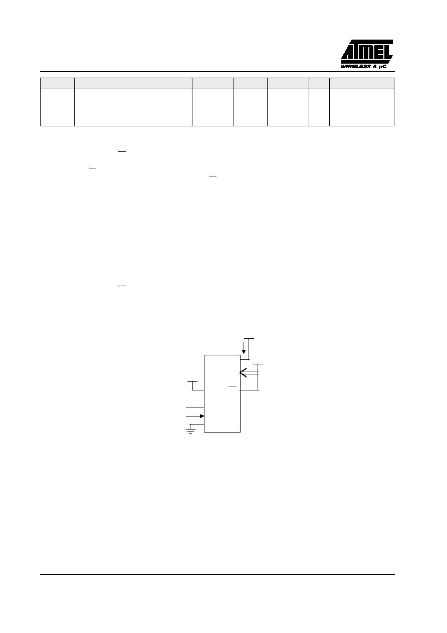
ICC under reset is measured with all output pins disconnected; XTAL1 driven with TCLCH, TCHCL = 5 ns (see Figure 24.), VIL = VSS + 0.5 V,
VIH = VCC - 0.5V; XTAL2 N.C.; EA = RST = Port 0 = VCC. ICC would be slightly higher if a crystal oscillator used..
2.
Idle ICC is measured with all output pins disconnected; XTAL1 driven with TCLCH,TCHCL = 5 ns, VIL =VSS + 0.5 V, VIH =VCC - 0.5 V; XTAL2
3.
Power Down ICC is measured with all output pins disconnected; EA = VSS, PORT 0 = VCC; XTAL2 NC.; RST = VSS (see Figure 23.).
4.
Capacitance loading on Ports 0 and 2 may cause spurious noise pulses to be superimposed on the VOLs of ALE and Ports 1 and 3. The noise is
due to external bus capacitance discharging into the Port 0 and Port 2 pins when these pins make 1 to 0 transitions during bus operation. In the worst
cases (capacitive loading 100pF), the noise pulse on the ALE line may exceed 0.45V with maxi VOL peak 0.6V. A Schmitt Trigger use is not necessary.
5.
Typicals are based on a limited number of samples and are not guaranteed. The values listed are at room temperature and 5V.
6.
Under steady state (non-transient) conditions, IOL must be externally limited as follows:
Maximum IOL per port pin: 10 mA
Maximum IOL per 8-bit port:
Port 0: 26 mA
Ports 1, 2, 3 and 4 and 5 when available: 15 mA
Maximum total IOL for all output pins: 71 mA
If IOL exceeds the test condition, VOL may exceed the related specication. Pins are not guaranteed to sink current greater than the listed test conditions.
7.
For other values, please contact your sales ofce.
8.
Operating ICC is measured with all output pins disconnected; XTAL1 driven with TCLCH, TCHCL = 5 ns (see Figure 24.), VIL = VSS + 0.5 V,
VIH =VCC - 0.5V; XTAL2 N.C.; EA = Port 0 = VCC; RST = VSS. The internal ROM runs the code 80 FE (label: SJMP label). ICC would be slightly
higher if a crystal oscillator is used. Measurements are made with OTP products when possible, which is the worst case.
Figure 20. ICC Test Condition, under reset
ICC
idle
Power Supply Current Maximum values, X1
mode: (7)
0.15 Freq
(MHz) + 0.2
@12MHz 2
@16MHz 2.6
mA
VCC = 3.3 V
(2)
Symbol
Parameter
Min
Typ
Max
Unit
Test Conditions
EA
VCC
ICC
(NC)
CLOCK
SIGNAL
VCC
All other pins are disconnected.
RST
XTAL2
XTAL1
VSS
VCC
P0
相關(guān)PDF資料 |
PDF描述 |
|---|---|
| TS87C51RD2-MIMB | 8-BIT, OTPROM, 40 MHz, MICROCONTROLLER, PQFP64 |
| TS87C51RB2-EED | 8-BIT, OTPROM, MICROCONTROLLER, PQFP44 |
| TS87C51RD2-VIBD | 8-BIT, OTPROM, 40 MHz, MICROCONTROLLER, PQCC44 |
| TSA5526MDK-T | PLL FREQUENCY SYNTHESIZER, 1300 MHz, PDSO16 |
| TSB100008DS | 40 A, BARRIER STRIP TERMINAL BLOCK |
相關(guān)代理商/技術(shù)參數(shù) |
參數(shù)描述 |
|---|---|
| TS83C51RB2ZZZ-LCED | 制造商:未知廠家 制造商全稱:未知廠家 功能描述:Microcontroller |
| TS83C51RB2ZZZ-LCER | 制造商:未知廠家 制造商全稱:未知廠家 功能描述:Microcontroller |
| TS83C51RB2ZZZ-LIAD | 制造商:未知廠家 制造商全稱:未知廠家 功能描述:Microcontroller |
| TS83C51RB2ZZZ-LIBB | 制造商:未知廠家 制造商全稱:未知廠家 功能描述:Microcontroller |
| TS83C51RB2ZZZ-LIBD | 制造商:未知廠家 制造商全稱:未知廠家 功能描述:Microcontroller |
發(fā)布緊急采購,3分鐘左右您將得到回復(fù)。