- 您現(xiàn)在的位置:買賣IC網(wǎng) > PDF目錄103066 > TS5A3160DCKT (TEXAS INSTRUMENTS INC) 1-CHANNEL, SGL POLE DOUBLE THROW SWITCH, PDSO6 PDF資料下載
參數(shù)資料
| 型號(hào): | TS5A3160DCKT |
| 廠商: | TEXAS INSTRUMENTS INC |
| 元件分類: | 多路復(fù)用及模擬開(kāi)關(guān) |
| 英文描述: | 1-CHANNEL, SGL POLE DOUBLE THROW SWITCH, PDSO6 |
| 封裝: | GREEN, PLASTIC, SC-70, 6 PIN |
| 文件頁(yè)數(shù): | 6/29頁(yè) |
| 文件大小: | 716K |
| 代理商: | TS5A3160DCKT |
第1頁(yè)第2頁(yè)第3頁(yè)第4頁(yè)第5頁(yè)當(dāng)前第6頁(yè)第7頁(yè)第8頁(yè)第9頁(yè)第10頁(yè)第11頁(yè)第12頁(yè)第13頁(yè)第14頁(yè)第15頁(yè)第16頁(yè)第17頁(yè)第18頁(yè)第19頁(yè)第20頁(yè)第21頁(yè)第22頁(yè)第23頁(yè)第24頁(yè)第25頁(yè)第26頁(yè)第27頁(yè)第28頁(yè)第29頁(yè)
SCDS216A – OCTOBER 2005 – REVISED OCTOBER 2009 ............................................................................................................................................ www.ti.com
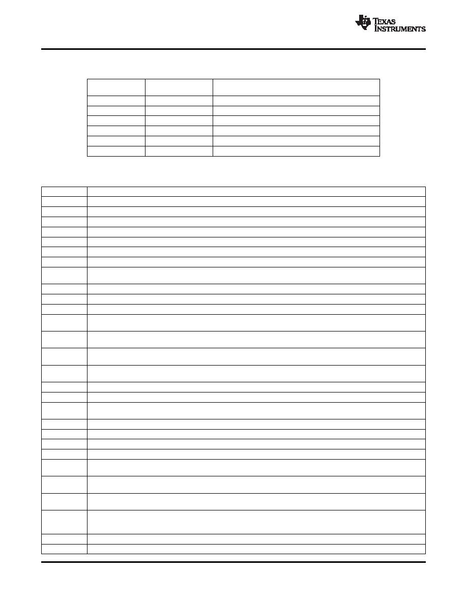
PIN DESCRIPTION
PIN
NAME
DESCRIPTION
NUMBER
1
NO
Normally open
2
GND
Digital ground
3
NC
Normally closed
4
COM
Common
5
V+
Power supply
6
IN
Digital control to connect COM to NO
PARAMETER DESCRIPTION
SYMBOL
DESCRIPTION
VCOM
Voltage at COM
VNC
Voltage at NC
VNO
Voltage at NO
ron
Resistance between COM and NO ports when the channel is ON
rpeak
Peak on-state resistance over a specified voltage range
Δron
Difference of ron between channels in a specific device
ron(flat)
Difference between the maximum and minimum value of ron in a channel over the specified range of conditions
Leakage current measured at the NC port, with the corresponding channel (NC to COM) in the OFF state under
INC(OFF)
worst-case input and output conditions
INC(PWROFF)
Leakage current measured at the NC port during the power-off condition, V+ = 0
INO(OFF)
Leakage current measured at the NO port, with the corresponding channel (NO to COM) in the OFF state
INO(PWROFF)
Leakage current measured at the NO port during the power-off condition, V+ = 0
Leakage current measured at the NC port, with the corresponding channel (NC to COM) in the ON state and the output
INC(ON)
(COM) open
Leakage current measured at the NO port, with the corresponding channel (NO to COM) in the ON state and the output
INO(ON)
(COM) open
Leakage current measured at the NO port, with the corresponding channel (NO to COM) in the OFF state and the output
INO(OFF)
(COM) open
Leakage current measured at the NO port, with the corresponding channel (NO to COM) in the ON state and the output
INO(ON)
(COM) open
ICOM(OFF)
Leakage current measured at the COM port, with the corresponding channel (COM to NO) in the OFF state
ICOM(PWROFF)
Leakage current measured at the COM port during the power-off condition, V+ = 0
Leakage current measured at the COM port, with the corresponding channel (COM to NO) in the ON state and the output
ICOM(ON)
(NO) open
VIH
Minimum input voltage for logic high for the control input (IN)
VIL
Maximum input voltage for logic low for the control input (IN)
VI
Voltage at the control input (IN)
IIH, IIL
Leakage current measured at the control input (IN)
Turn-on time for the switch. This parameter is measured under the specified range of conditions and by the propagation
tON
delay between the digital control (IN) signal and analog output (COM or NO) signal when the switch is turning ON.
Turn-off time for the switch. This parameter is measured under the specified range of conditions and by the propagation
tOFF
delay between the digital control (IN) signal and analog output (COM or NO) signal when the switch is turning OFF.
Make-before-break time. This parameter is measured under the specified range of conditions and by the propagation delay
tMBB
between the output of two adjacent analog channels (NC and NO) when the control signal changes state.
Charge injection is a measurement of unwanted signal coupling from the control (IN) input to the analog (NO or COM)
QC
output. This is measured in coulomb (C) and measured by the total charge induced due to switching of the control
input.Charge injection, QC = CL × ΔVCOM, CL is the load capacitance and ΔVCOM is the change in analog output voltage.
CNC(OFF)
Capacitance at the NC port when the corresponding channel (NC to COM) is OFF
CNO(OFF)
Capacitance at the NO port when the corresponding channel (NO to COM) is OFF
14
Copyright 2005–2009, Texas Instruments Incorporated
Product Folder Link(s): TS5A3160
相關(guān)PDF資料 |
PDF描述 |
|---|---|
| TPS62400DRCTG4 | 0.6 A DUAL SWITCHING CONTROLLER, 2500 kHz SWITCHING FREQ-MAX, PDSO10 |
| TL4050A10IDCKR | 1-OUTPUT TWO TERM VOLTAGE REFERENCE, 10 V, PDSO5 |
| TL4050C25QDBZT | 1-OUTPUT TWO TERM VOLTAGE REFERENCE, 2.5 V, PDSO3 |
| TL4050C25IDBZTG4 | 1-OUTPUT TWO TERM VOLTAGE REFERENCE, 2.5 V, PDSO3 |
| TPS2556DRB | 1-CHANNEL POWER SUPPLY SUPPORT CKT, PDSO8 |
相關(guān)代理商/技術(shù)參數(shù) |
參數(shù)描述 |
|---|---|
| TS5A3160DCKTE4 | 功能描述:模擬開(kāi)關(guān) IC 1O SPDT Ana Sw RoHS:否 制造商:Texas Instruments 開(kāi)關(guān)數(shù)量:2 開(kāi)關(guān)配置:SPDT 開(kāi)啟電阻(最大值):0.1 Ohms 切換電壓(最大): 開(kāi)啟時(shí)間(最大值): 關(guān)閉時(shí)間(最大值): 工作電源電壓:2.7 V to 4.5 V 最大工作溫度:+ 85 C 安裝風(fēng)格:SMD/SMT 封裝 / 箱體:DSBGA-16 |
| TS5A3160DCKTG4 | 功能描述:模擬開(kāi)關(guān) IC 1O SPDT Ana Sw RoHS:否 制造商:Texas Instruments 開(kāi)關(guān)數(shù)量:2 開(kāi)關(guān)配置:SPDT 開(kāi)啟電阻(最大值):0.1 Ohms 切換電壓(最大): 開(kāi)啟時(shí)間(最大值): 關(guān)閉時(shí)間(最大值): 工作電源電壓:2.7 V to 4.5 V 最大工作溫度:+ 85 C 安裝風(fēng)格:SMD/SMT 封裝 / 箱體:DSBGA-16 |
| TS5A3160YEPR | 制造商:TI 制造商全稱:Texas Instruments 功能描述:1-ohm SPDT ANALOG SWITCH 5-V/3.3-V SINGLE-CHANNEL 2:1 MULTIPLEXER/DEMULTIPLEXER |
| TS5A3160YZPR | 制造商:TI 制造商全稱:Texas Instruments 功能描述:1-ohm SPDT ANALOG SWITCH 5-V/3.3-V SINGLE-CHANNEL 2:1 MULTIPLEXER/DEMULTIPLEXER |
| TS5A3166 | 制造商:NSC 制造商全稱:National Semiconductor 功能描述:0.9-OHM SPST ANALOG SWITCH |
發(fā)布緊急采購(gòu),3分鐘左右您將得到回復(fù)。