- 您現(xiàn)在的位置:買賣IC網(wǎng) > PDF目錄98285 > TPS65055RSMR (TEXAS INSTRUMENTS INC) 1.8 A DUAL SWITCHING CONTROLLER, 2475 kHz SWITCHING FREQ-MAX, PQCC32 PDF資料下載
參數(shù)資料
| 型號: | TPS65055RSMR |
| 廠商: | TEXAS INSTRUMENTS INC |
| 元件分類: | 穩(wěn)壓器 |
| 英文描述: | 1.8 A DUAL SWITCHING CONTROLLER, 2475 kHz SWITCHING FREQ-MAX, PQCC32 |
| 封裝: | 4 X 4 MM, GREEN, PLASTIC, QFN-32 |
| 文件頁數(shù): | 13/41頁 |
| 文件大?。?/td> | 1276K |
| 代理商: | TPS65055RSMR |
第1頁第2頁第3頁第4頁第5頁第6頁第7頁第8頁第9頁第10頁第11頁第12頁當(dāng)前第13頁第14頁第15頁第16頁第17頁第18頁第19頁第20頁第21頁第22頁第23頁第24頁第25頁第26頁第27頁第28頁第29頁第30頁第31頁第32頁第33頁第34頁第35頁第36頁第37頁第38頁第39頁第40頁第41頁
Under-Voltage Lockout
ENABLE
discharge
threshold
Vbat
Vref=1V
+
-
Vbat
threshold
discharge
RST and DPD
SHORT-CIRCUIT PROTECTION
SLVS844 – SEPTEMBER 2008.......................................................................................................................................................................................... www.ti.com
The under voltage lockout circuit prevents the device from malfunctioning at low input voltages and from
excessive discharge of the battery and disables the converters and LDOs. The under-voltage lockout threshold is
typically 1.8 V.
The DCDC converters and the LDOs are enabled using external enable pins or enable bits with the I2C
compatible interface. The signal of the enable pin and the enable bit are logically XORed to generate the enable
signal to the converter or LDO. There is one enable pin and one enable bit for each of the LDOs or DCDC
converters, which allows start up of each converter independently. If EN_DCDC1, EN_DCDC2, EN_LDO1,
EN_LDO2, ENLDO3, or EN_LDO4 are set to high, the corresponding converter starts up with soft start as
previously described. The converters and LDOs can also be enabled by setting the enable bits for each of the
LDOs or DCDC converters in register REG_CTRL. See the register description for more details.
Disabling the DCDC converter or LDO forces the device into shutdown with a shutdown quiescent current as
defined in the electrical characteristics. In this mode, the P and N-Channel MOSFETs are turned-off, and the
entire internal control circuitry is switched-off. For proper operation the enable pins must be terminated and must
not be left floating.
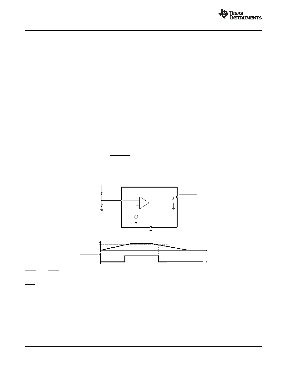
The TPS65055 contains a comparator that supervises a voltage applied to the threshold pin and drives a open
drain NMOS according to the input level applied at threshold. If the input voltage at the threshold pin is lower
than 1V, the open drain NMOS at the discharge output is turned on, pulling the pin to GND. This circuitry is
functional as soon as the supply voltage at Vcc exceeds the undervoltage lockout threshold. Therefore the
TPS65055 has a shutdown current (all DCDC converters and LDOs are off) of 9
A in order to supply bandgap
and comparator.
The TPS65055 contains two open drain outputs that are controlled by the I2C compatible interface. The RST and
DPD outputs are low (internal NMOS active) per default, once the undervoltage lockout threshold has been
exceeded. The status of these outputs can be changed using the REG_CTRL register. See the register
description for more details.
All outputs are short-circuit protected with a maximum output current as defined in the electrical specifications.
20
Copyright 2008, Texas Instruments Incorporated
Product Folder Link(s): TPS65055
相關(guān)PDF資料 |
PDF描述 |
|---|---|
| TPS65058RGET | 1.8 A DUAL SWITCHING CONTROLLER, 2475 kHz SWITCHING FREQ-MAX, PQCC32 |
| TPS650732TRSLRQ1 | POWER SUPPLY SUPPORT CKT, PQCC48 |
| TPS65110RGEG3 | SWITCHED CAPACITOR REGULATOR, 520 kHz SWITCHING FREQ-MAX, PQCC24 |
| TPS65130RGER | 0.9 A SWITCHING REGULATOR, 1500 kHz SWITCHING FREQ-MAX, PQCC24 |
| TPS65130RGET | 0.9 A SWITCHING REGULATOR, 1500 kHz SWITCHING FREQ-MAX, PQCC24 |
相關(guān)代理商/技術(shù)參數(shù) |
參數(shù)描述 |
|---|---|
| TPS65055RSMRG4 | 功能描述:PMIC 解決方案 Dual buck w/ 4LDO & I2C RoHS:否 制造商:Texas Instruments 安裝風(fēng)格:SMD/SMT 封裝 / 箱體:QFN-24 封裝:Reel |
| TPS65055RSMT | 功能描述:PMIC 解決方案 Dual buck w/ 4LDO & I2C RoHS:否 制造商:Texas Instruments 安裝風(fēng)格:SMD/SMT 封裝 / 箱體:QFN-24 封裝:Reel |
| TPS65055RSMTG4 | 功能描述:PMIC 解決方案 Dual buck w/ 4LDO & I2C RoHS:否 制造商:Texas Instruments 安裝風(fēng)格:SMD/SMT 封裝 / 箱體:QFN-24 封裝:Reel |
| TPS65056EVM-195 | 功能描述:電源管理IC開發(fā)工具 TPS65056 Eval Mod RoHS:否 制造商:Maxim Integrated 產(chǎn)品:Evaluation Kits 類型:Battery Management 工具用于評估:MAX17710GB 輸入電壓: 輸出電壓:1.8 V |
| TPS65056RSMR | 功能描述:PMIC 解決方案 6Ch Pwr Mgmt IC RoHS:否 制造商:Texas Instruments 安裝風(fēng)格:SMD/SMT 封裝 / 箱體:QFN-24 封裝:Reel |
發(fā)布緊急采購,3分鐘左右您將得到回復(fù)。