- 您現(xiàn)在的位置:買(mǎi)賣(mài)IC網(wǎng) > PDF目錄384025 > TP3064BN (Texas Instruments, Inc.) MONOLITHIC SERIAL INTERFACE COMBINED PCM CODEC AND FILTER PDF資料下載
參數(shù)資料
| 型號(hào): | TP3064BN |
| 廠商: | Texas Instruments, Inc. |
| 元件分類(lèi): | Codec |
| 英文描述: | MONOLITHIC SERIAL INTERFACE COMBINED PCM CODEC AND FILTER |
| 中文描述: | 整體式串行接口的PCM編解碼器和過(guò)濾器 |
| 文件頁(yè)數(shù): | 3/21頁(yè) |
| 文件大小: | 300K |
| 代理商: | TP3064BN |
第1頁(yè)第2頁(yè)當(dāng)前第3頁(yè)第4頁(yè)第5頁(yè)第6頁(yè)第7頁(yè)第8頁(yè)第9頁(yè)第10頁(yè)第11頁(yè)第12頁(yè)第13頁(yè)第14頁(yè)第15頁(yè)第16頁(yè)第17頁(yè)第18頁(yè)第19頁(yè)第20頁(yè)第21頁(yè)
TP3064B, TP3067B, TP13064B, TP13067B
MONOLITHIC SERIAL INTERFACE
COMBINED PCMCODEC AND FILTER
SCTS031D – MAY 1990 –REVISED JULY 1996
3
POST OFFICE BOX 655303
DALLAS, TEXAS 75265
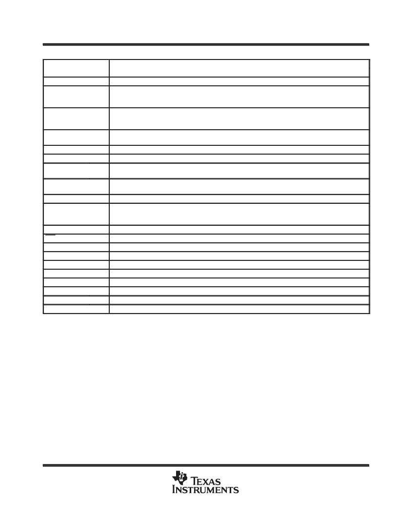
Terminal Functions
TERMINAL
NAME
ANLG GND
DESCRIPTION
NO.
2
Analog ground. All signals are referenced to ANLG GND.
ANLG LOOP
16
Analog loopback control input. Must be set to logic low for normal operation. When pulled to logic high, the transmit
filter input is disconnected from the output of the transmit preamplifier and connected to the VPO+ output of the
receive power amplifier.
BCLKR/CLKSEL
9
The bit clock that shifts data into DR after the FSR leading edge. May vary from 64 kHz to 2.048 MHz. Alternately,
can be a logic input that selects either 1.536 MHz/1.544 MHz or 2.048 MHz for master clock in synchronous mode.
BCLKX is used for both transmit and receive directions (see Table 1).
BCLKX
12
The bit clock that shifts out the PCM data on DX. May vary from 64 kHz to 2.048 MHz, but must be synchronous
with MCLKX
DR
8
Receive data input. PCM data is shifted into DR following the FSR leading edge.
DX
13
The 3-state PCM data output that is enabled by FSX
FSR
7
Receive frame-sync pulse input that enables BCLKR to shift PCM data in DR. FSR is an 8-kHz pulse train (see
Figures 1 and 2 for timing details).
FSX
14
Transmit frame-sync pulse that enables BCLKX to shift out the PCM data on DX. FSX is an 8-kHz pulse train (see
Figures 1 and 2 for timing details).
GSX
17
Analog output of the transmit input amplifier. GSX is used to externally set gain.
MCLKR/PDN
10
Receive master clock (must be 1.536 MHz, 1.544 MHz, or 2.048 MHz). May be synchronous with MCLKX, but
should be synchronous for best performance. When MCLKR is connected continuously low, MCLKX is selected
for all internal timing. When MCLKR is connected continuously high, the device is powered down.
MCLKX
11
Transmit master clock (must be 1.536 MHz, 1.544 MHz, or 2.048 MHz). May be asynchronous with MCLKR
TSX
15
Open-drain output that pulses low during the encoder time slot
Negative power supply. VBB = –5 V
±
5%
Positive power supply. VCC = 5 V
±
5%
Analog output of the receive filter
VBB
VCC
VFRO
20
6
5
VFXI+
19
Noninverting input of the transmit input amplifier
VFXI–
18
Inverting input of the transmit input amplifier
VPI
4
Inverting input to the receive power amplifier. Also powers down both amplifiers when connected to VBB.
The noninverted output of the receive power amplifier
VPO+
1
VPO–
3
The inverted output of the receive power amplifier
相關(guān)PDF資料 |
PDF描述 |
|---|---|
| TP3067B | MONOLITHIC SERIAL INTERFACE COMBINED PCM CODEC AND FILTER |
| TP13064B | MONOLITHIC SERIAL INTERFACE COMBINED PCM CODEC AND FILTER |
| TP13064BDW | MONOLITHIC SERIAL INTERFACE COMBINED PCM CODEC AND FILTER |
| TP13064BN | MONOLITHIC SERIAL INTERFACE COMBINED PCM CODEC AND FILTER |
| TP13067B | MONOLITHIC SERIAL INTERFACE COMBINED PCM CODEC AND FILTER |
相關(guān)代理商/技術(shù)參數(shù) |
參數(shù)描述 |
|---|---|
| TP3064BW | 制造商:Texas Instruments 功能描述: |
| TP3064J | 制造商:NSC 制造商全稱(chēng):National Semiconductor 功能描述:``Enhanced' Serial Interface CMOS CODEC/Filter COMBO |
| TP3064N | 制造商:NSC 制造商全稱(chēng):National Semiconductor 功能描述:``Enhanced' Serial Interface CMOS CODEC/Filter COMBO |
| TP3064V | 制造商:NSC 制造商全稱(chēng):National Semiconductor 功能描述:``Enhanced' Serial Interface CMOS CODEC/Filter COMBO |
| TP3064V/A+ | 制造商:未知廠家 制造商全稱(chēng):未知廠家 功能描述:u-Law CODEC |
發(fā)布緊急采購(gòu),3分鐘左右您將得到回復(fù)。