- 您現(xiàn)在的位置:買賣IC網(wǎng) > PDF目錄384025 > TP13067BN (Texas Instruments, Inc.) MONOLITHIC SERIAL INTERFACE COMBINED PCM CODEC AND FILTER PDF資料下載
參數(shù)資料
| 型號: | TP13067BN |
| 廠商: | Texas Instruments, Inc. |
| 元件分類: | Codec |
| 英文描述: | MONOLITHIC SERIAL INTERFACE COMBINED PCM CODEC AND FILTER |
| 中文描述: | 整體式串行接口的PCM編解碼器和過濾器 |
| 文件頁數(shù): | 8/21頁 |
| 文件大小: | 300K |
| 代理商: | TP13067BN |
TP3064B, TP3067B, TP13064B, TP13067B
MONOLITHIC SERIAL INTERFACE
COMBINED PCMCODEC AND FILTER
SCTS031D – MAY 1990 –REVISED JULY 1996
8
POST OFFICE BOX 655303
DALLAS, TEXAS 75265
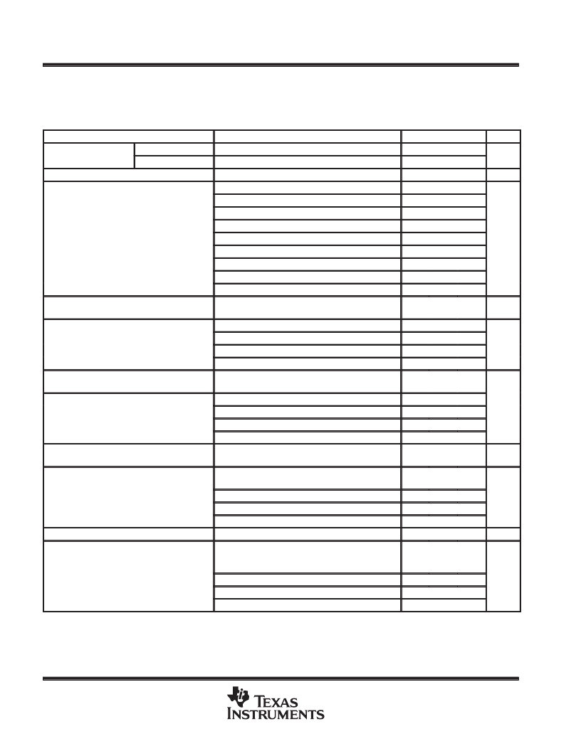
operating characteristics over operating free-air temperature range, V
CC
= 5 V
±
5%,
V
BB
= –5 V
±
5%, GND at 0 V, V
I
= 1.2276 V, f = 1.02 kHz, transmit input amplifier connected for unity
gain, noninverting (unless otherwise noted)
filter gains and tracking errors
PARAMETER
TEST CONDITIONS
MIN
TYP
2.501
MAX
UNIT
Maximum peak transmit
overload level
TP3064B, TP13064B
3.17 dBm0
V
TP3067B, TP13067B
3.14 dBm0
TA = 25
°
C
f = 16 Hz
2.492
Transmit filter gain, absolute (at 0 dBm0)
–0.15
0.15
dB
–40
f = 50 Hz
–30
f = 60 Hz
–26
f = 200 Hz
–1.8
–0.1
Transmit filter gain, relative to absolute
f = 300 Hz to 3000 Hz
–0.15
0.15
dB
f = 3300 Hz
–0.35
0.05
f = 3400 Hz
–0.8
0
f = 4000 Hz
f
≥
4600 Hz (measure response from 0 Hzto4000Hz)
–14
–32
Absolute transmit gain variation with
temperature and supply voltage
Relative to absolute transmit gain
–0.1
0.1
dB
Sinusoidal test method; Reference level = –10 dBm0
3 dBm0
≥
input level
≥
–40 dBm0
–40 dBm0 > input level
≥
–50 dBm0
–50 dBm0 > input level
≥
–55 dBm0
Input is digital code sequence for 0 dBm0 signal,
TA = 25
°
C
f = 0 Hz to 3000 Hz,
Transmit gain tracking error with level
±
0.2
±
0.4
±
0.8
dB
Receive filter gain, absolute (at 0 dBm0)
–0.15
0.15
dB
TA = 25
°
C
–0.15
0.15
Receive filter gain relative to absolute
Receive filter gain, relative to absolute
f = 3300 Hz
–0.35
0.05
dB
f = 3400 Hz
–0.8
0
f = 4000 Hz
–14
Absolute receive gain variation with temperature
and supply voltage
TA = full range,
See Note 4
–0.1
0.1
dB
Sinusoidal test method; reference input PCM code
corresponds to an ideally encoded –10 dBm0 signal
3 dBm0
≥
input level
≥
–40 dBm0
–40 dBm0 > input level
≥
–50 dBm0
–50 dBm0 > input level
≥
–55 dBm0
RL = 10 k
Pseudo-noise test method; reference input PCM
code corresponds to an ideally encoded –10 dBm0
signal
3 dBm0
≥
input level
≥
–40 dBm0
–40 dBm0 > input level
≥
–50 dBm0
–50 dBm0 > input level
≥
–55 dBm0
Receive gain tracking error with level
±
0.2
±
0.4
±
0.8
±
2.5
dB
Receive output drive voltage
V
Transmit and receive gain tracking error with
level (A-law, CCITT C712)
±
0.25
±
0.3
±
0.45
dB
All typical values are at VCC = 5 V, VBB = –5 V, and TA = 25
°
C.
Absolute rms signal levels are defined as follows: VI = 1.2276 V = 0 dBm0 = 4 dBm at f = 1.02 kHz with RL = 600
.
NOTE 4: Full range for the TP3064B and TP3067B is 0
°
C to 70
°
C. Full range for the TP13064B and TP13067B is –40
°
C to 85
°
C.
相關(guān)PDF資料 |
PDF描述 |
|---|---|
| TP3064B | MONOLITHIC SERIAL INTERFACE COMBINED PCM CODEC AND FILTER |
| TP3064BDW | MONOLITHIC SERIAL INTERFACE COMBINED PCM CODEC AND FILTER |
| TP3064BN | MONOLITHIC SERIAL INTERFACE COMBINED PCM CODEC AND FILTER |
| TP3067B | MONOLITHIC SERIAL INTERFACE COMBINED PCM CODEC AND FILTER |
| TP13064B | MONOLITHIC SERIAL INTERFACE COMBINED PCM CODEC AND FILTER |
相關(guān)代理商/技術(shù)參數(shù) |
參數(shù)描述 |
|---|---|
| TP130K | 功能描述:鉗型萬用表及配件 AIR/GAS K TYPE PROBE RoHS:否 制造商:Fluke 準(zhǔn)確性:2 % 測距:400 A |
| TP130KA | 功能描述:測試探頭 AIR/GAS PROBE K TYPE RoHS:否 制造商:Teledyne LeCroy 設(shè)備類型:Passive Probes 帶寬:500 MHz 尖端類型: 長度:1.3 mm 顏色:Black 電壓額定值: 電流額定值: |
| TP1311 | 制造商:未知廠家 制造商全稱:未知廠家 功能描述:Analog IC |
| TP1312 | 制造商:未知廠家 制造商全稱:未知廠家 功能描述:Analog IC |
| TP1313 | 制造商:未知廠家 制造商全稱:未知廠家 功能描述:Analog IC |
發(fā)布緊急采購,3分鐘左右您將得到回復(fù)。