- 您現(xiàn)在的位置:買賣IC網(wǎng) > PDF目錄383961 > TN83C196MD (Intel Corp.) INDUSTRIAL MOTOR CONTROL MICROCONTROLLER PDF資料下載
參數(shù)資料
| 型號(hào): | TN83C196MD |
| 廠商: | Intel Corp. |
| 英文描述: | INDUSTRIAL MOTOR CONTROL MICROCONTROLLER |
| 中文描述: | 工業(yè)電機(jī)控制微控制器 |
| 文件頁數(shù): | 21/25頁 |
| 文件大小: | 1062K |
| 代理商: | TN83C196MD |
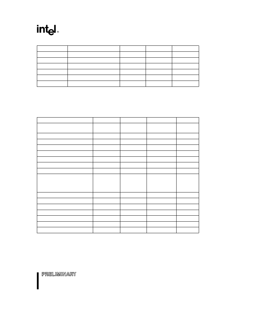
8XC196MD
8-BIT MODE A/D OPERATING CONDITIONS
Symbol
Description
Min
Max
Units
§
C
T
A
Ambient Temperature
b
40
a
85
V
CC
Digital Supply Voltage
4.50
5.50
V
V
REF
Analog Supply Voltage
4.00
5.50
V
(1)
T
SAM
Sample Time
1.0
m
s
(2)
T
CONV
Conversion Time
7.0
20.0
m
s
(2)
F
OSC
Oscillator Frequency
8.0
16.0
MHz
NOTES:
ANGND and V
SS
should nominally be at the same potential.
1. V
must be within 0.5V of V
.
2. The value of ADDTIME is selected to meet these specifications.
8-BIT MODE A/D CHARACTERISTICS
(Over the Above Operating Conditions)
Parameter
Typical
(1)
Min
Max
Units
*
Resolution
256
8
256
8
Level
Bits
Absolute Error
0
g
1
LSBs
Full Scale Error
g
0.5
LSBs
Zero Offset Error
g
0.5
LSBs
Non-Linearity
0
g
1
LSBs
Differential Non-Linearity
l
b
1
a
1
LSBs
Channel-to-Channel Matching
0
g
1.0
LSBs
Repeatability
g
0.25
LSBs
Temperature Coefficients:
Offset
Full Scale
Differential Non-Linearity
0.003
0.003
0.003
LSB/C
LSB/C
LSB/C
Off Isolation
b
60
dB
(2, 3)
Feedthrough
b
60
dB
(2)
V
CC
Power Supply Rejection
b
60
dB
(2)
Input Series Resistance
750
2K
X
(4)
Voltage on Analog Input Pin
V
SS
b
0.5
V
REF
a
0.5
V
(5, 6)
Sampling Capacitor
3
pF
DC Input Leakage
g
1
0
g
3.0
m
A
NOTES:
*
An ‘‘LSB’’ as used here, has a value of approximately 20 mV. (See Embedded Microcontrollers and Processors Handbook
for A/D glossary of terms).
1. These values are expected for most parts at 25
§
C but are not tested or guaranteed.
2. DC to 100 KHz.
3. Multiplexer Break-Before-Make is guaranteed.
4. Resistance from device pin, through internal MUX, to sample capacitor.
5. These values may be exceeded if the pin current is limited to
g
2 mA.
6. Applying voltages beyond these specifications will degrade the accuracy of other channels being converted.
7. All conversions performed with processor in IDLE mode.
21
相關(guān)PDF資料 |
PDF描述 |
|---|---|
| TND009T | CONNECTOR ACCESSORY |
| TND010F | CONNECTOR ACCESSORY |
| TND011MP | CONNECTOR ACCESSORY |
| TND011NM | CONNECTOR ACCESSORY |
| TND012MP | Low-Side Power Switch for Use in Solenoid,Lamp Drive Applications |
相關(guān)代理商/技術(shù)參數(shù) |
參數(shù)描述 |
|---|---|
| TN83C198 | 制造商:未知廠家 制造商全稱:未知廠家 功能描述:16-Bit Microcontroller |
| TN83C198-16 | 制造商:未知廠家 制造商全稱:未知廠家 功能描述:16-Bit Microcontroller |
| TN83C251SA16 | 制造商:INTEL 制造商全稱:Intel Corporation 功能描述:HIGH-PERFORMANCE CHMOS MICROCONTROLLER |
| TN83C251SB | 制造商:未知廠家 制造商全稱:未知廠家 功能描述:8-Bit Microcontroller |
| TN83C251SB16 | 制造商:INTEL 制造商全稱:Intel Corporation 功能描述:HIGH-PERFORMANCE CHMOS MICROCONTROLLER |
發(fā)布緊急采購(gòu),3分鐘左右您將得到回復(fù)。