- 您現(xiàn)在的位置:買賣IC網(wǎng) > PDF目錄384024 > TN80L186EB8 (INTEL CORP) 16-BIT HIGH-INTEGRATION EMBEDDED PROCESSORS PDF資料下載
參數(shù)資料
| 型號: | TN80L186EB8 |
| 廠商: | INTEL CORP |
| 元件分類: | 微控制器/微處理器 |
| 英文描述: | 16-BIT HIGH-INTEGRATION EMBEDDED PROCESSORS |
| 中文描述: | 16-BIT, 8 MHz, MICROPROCESSOR, PQCC84 |
| 封裝: | PLASTIC, LCC-84 |
| 文件頁數(shù): | 11/59頁 |
| 文件大?。?/td> | 779K |
| 代理商: | TN80L186EB8 |
第1頁第2頁第3頁第4頁第5頁第6頁第7頁第8頁第9頁第10頁當前第11頁第12頁第13頁第14頁第15頁第16頁第17頁第18頁第19頁第20頁第21頁第22頁第23頁第24頁第25頁第26頁第27頁第28頁第29頁第30頁第31頁第32頁第33頁第34頁第35頁第36頁第37頁第38頁第39頁第40頁第41頁第42頁第43頁第44頁第45頁第46頁第47頁第48頁第49頁第50頁第51頁第52頁第53頁第54頁第55頁第56頁第57頁第58頁第59頁
80C186EB/80C188EB, 80L186EB/80L188EB
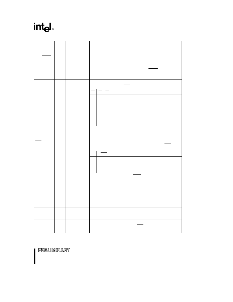
Table 3. Pin Descriptions
(Continued)
Pin
Name
Pin
Type
Input
Type
Output
States
Description
A18:16
A19/ONCE
(A15:A8)
(A18:16)
(A19/ONCE)
I/O
A(L)
H(Z)
R(WH)
P(X)
These pins provide multiplexed
Address
during the address
phase of the bus cycle. Address bits 16 through 19 are presented
on these pins and can be latched using ALE. These pins are
driven to a logic 0 during the data phase of the bus cycle. On the
80C188EB, A15–A8 provide valid address information for the
entire bus cycle. During a processor reset (RESIN active), A19/
ONCE is used to enable ONCE mode. A18:16 must not be driven
low during reset or improper operation may result.
S2:0
O
D
H(Z)
R(Z)
P(1)
Bus cycle
Status
are encoded on these pins to provide bus
transaction information. S2:0 are encoded as follows:
S2
S1
S0
Bus Cycle Initiated
0
0
0
0
1
1
1
1
0
0
1
1
0
0
1
1
0
1
0
1
0
1
0
1
Interrupt Acknowledge
Read I/O
Write I/O
Processor HALT
Queue Instruction Fetch
Read Memory
Write Memory
Passive (no bus activity)
ALE
O
D
H(0)
R(0)
P(0)
Address Latch Enable
output is used to strobe address
information into a transparent type latch during the address phase
of the bus cycle.
BHE
(RFSH)
O
D
H(Z)
R(Z)
P(X)
Byte High Enable
output to indicate that the bus cycle in progress
is transferring data over the upper half of the data bus. BHE and
A0 have the following logical encoding
A0
BHE
Encoding
(for the 80C186EB/80L186EB only)
0
0
1
1
0
1
0
1
Word Transfer
Even Byte Transfer
Odd Byte Transfer
Refresh Operation
On the 80C188EB/80L188EB, RFSH is asserted low to indicate a
refresh bus cycle.
RD
O
D
H(Z)
R(Z)
P(1)
ReaD
output signals that the accessed memory or I/O device
must drive data information onto the data bus.
WR
O
D
H(Z)
R(Z)
P(1)
WRite
output signals that data available on the data bus are to be
written into the accessed memory or I/O device.
READY
I
A(L)
S(L)
D
READY
input to signal the completion of a bus cycle. READY
must be active to terminate any bus cycle, unless it is ignored by
correctly programming the Chip-Select Unit.
DEN
O
D
H(Z)
R(Z)
P(1)
Data ENable
output to control the enable of bi-directional
transceivers in a buffered system. DEN is active only when data is
to be transferred on the bus.
NOTE:
Pin names in parentheses apply to the 80C188EB/80L188EB.
11
11
相關(guān)PDF資料 |
PDF描述 |
|---|---|
| TN80L188EB13 | 16-BIT HIGH-INTEGRATION EMBEDDED PROCESSORS |
| TN80L188EB16 | 16-BIT HIGH-INTEGRATION EMBEDDED PROCESSORS |
| TN87C198 | COMMERCIAL/EXPRESS CHMOS MICROCONTROLLER |
| TN8xC198 | COMMERCIAL/EXPRESS CHMOS MICROCONTROLLER |
| TNC-BPJ-1.5WCR(A) | RFCO-AXIAL CONNECTORS |
相關(guān)代理商/技術(shù)參數(shù) |
參數(shù)描述 |
|---|---|
| TN80L186EB-8 | 制造商:未知廠家 制造商全稱:未知廠家 功能描述:16-Bit Microprocessor |
| TN80L188EA13 | 功能描述:IC MPU 16-BIT 3V 13MHZ 68-PLCC RoHS:否 類別:集成電路 (IC) >> 嵌入式 - 微處理器 系列:- 標準包裝:2 系列:MPC8xx 處理器類型:32-位 MPC8xx PowerQUICC 特點:- 速度:133MHz 電壓:3.3V 安裝類型:表面貼裝 封裝/外殼:357-BBGA 供應(yīng)商設(shè)備封裝:357-PBGA(25x25) 包裝:托盤 |
| TN80L188EA-13 | 制造商:未知廠家 制造商全稱:未知廠家 功能描述:16-Bit Microprocessor |
| TN80L188EA-8 | 制造商:未知廠家 制造商全稱:未知廠家 功能描述:16-Bit Microprocessor |
| TN80L188EB13 | 功能描述:IC MPU 16-BIT 3V 13MHZ 84-PLCC RoHS:否 類別:集成電路 (IC) >> 嵌入式 - 微處理器 系列:- 標準包裝:2 系列:MPC8xx 處理器類型:32-位 MPC8xx PowerQUICC 特點:- 速度:133MHz 電壓:3.3V 安裝類型:表面貼裝 封裝/外殼:357-BBGA 供應(yīng)商設(shè)備封裝:357-PBGA(25x25) 包裝:托盤 |
發(fā)布緊急采購,3分鐘左右您將得到回復。