- 您現(xiàn)在的位置:買賣IC網(wǎng) > PDF目錄384024 > TN80C188EB25 (INTEL CORP) 16-BIT HIGH-INTEGRATION EMBEDDED PROCESSORS PDF資料下載
參數(shù)資料
| 型號(hào): | TN80C188EB25 |
| 廠商: | INTEL CORP |
| 元件分類: | 微控制器/微處理器 |
| 英文描述: | 16-BIT HIGH-INTEGRATION EMBEDDED PROCESSORS |
| 中文描述: | 16-BIT, 25 MHz, MICROPROCESSOR, PQCC84 |
| 封裝: | PLASTIC, LCC-84 |
| 文件頁數(shù): | 10/59頁 |
| 文件大小: | 779K |
| 代理商: | TN80C188EB25 |
第1頁第2頁第3頁第4頁第5頁第6頁第7頁第8頁第9頁當(dāng)前第10頁第11頁第12頁第13頁第14頁第15頁第16頁第17頁第18頁第19頁第20頁第21頁第22頁第23頁第24頁第25頁第26頁第27頁第28頁第29頁第30頁第31頁第32頁第33頁第34頁第35頁第36頁第37頁第38頁第39頁第40頁第41頁第42頁第43頁第44頁第45頁第46頁第47頁第48頁第49頁第50頁第51頁第52頁第53頁第54頁第55頁第56頁第57頁第58頁第59頁
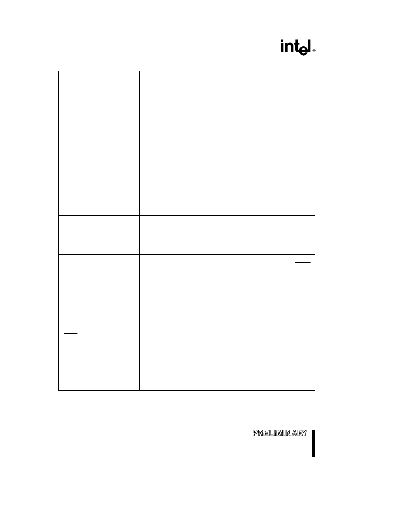
80C186EB/80C188EB, 80L186EB/80L188EB
Table 3. Pin Descriptions
Pin
Name
Pin
Type
Input
Type
Output
States
Description
V
CC
P
D
D
POWER
connections consist of four pins which must be
shorted externally to a V
CC
board plane.
V
SS
G
D
D
GROUND
connections consist of six pins which must be
shorted externally to a V
SS
board plane.
CLKIN
I
A(E)
D
CLocK INput
is an input for an external clock. An external
oscillator operating at two times the required processor
operating frequency can be connected to CLKIN. For crystal
operation, CLKIN (along with OSCOUT) are the crystal
connections to an internal Pierce oscillator.
OSCOUT
O
D
H(Q)
R(Q)
P(Q)
OSCillator OUTput
is only used when using a crystal to
generate the external clock. OSCOUT (along with CLKIN)
are the crystal connections to an internal Pierce oscillator.
This pin is not to be used as 2X clock output for non-crystal
applications (i.e., this pin is N.C. for non-crystal applications).
OSCOUT does not float in ONCE mode.
CLKOUT
O
D
H(Q)
R(Q)
P(Q)
CLocK OUTput
provides a timing reference for inputs and
outputs of the processor, and is one-half the input clock
(CLKIN) frequency. CLKOUT has a 50% duty cycle and
transistions every falling edge of CLKIN.
RESIN
I
A(L)
D
RESet IN
causes the processor to immediately terminate
any bus cycle in progress and assume an initialized state. All
pins will be driven to a known state, and RESOUT will also
be driven active. The rising edge (low-to-high) transition
synchronizes CLKOUT with CLKIN before the processor
begins fetching opcodes at memory location 0FFFF0H.
RESOUT
O
D
H(0)
R(1)
P(0)
RESet OUTput
that indicates the processor is currently in
the reset state. RESOUT will remain active as long as RESIN
remains active.
PDTMR
I/O
A(L)
H(WH)
R(Z)
P(1)
Power-Down TiMeR
pin (normally connected to an external
capacitor) that determines the amount of time the processor
waits after an exit from power down before resuming normal
operation. The duration of time required will depend on the
startup characteristics of the crystal oscillator.
NMI
I
A(E)
D
Non-Maskable Interrupt
input causes a TYPE-2 interrupt to
be serviced by the CPU. NMI is latched internally.
TEST/BUSY
(TEST)
I
A(E)
D
TEST
is used during the execution of the WAIT instruction to
suspend CPU operation until the pin is sampled active
(LOW). TEST is alternately known as BUSY when interfacing
with an 80C187 numerics coprocessor (80C186EB only).
AD15:0
(AD7:0)
I/O
S(L)
H(Z)
R(Z)
P(X)
These pins provide a multiplexed
Address
and
Data
bus.
During the address phase of the bus cycle, address bits 0
through 15 (0 through 7 on the 80C188EB) are presented on
the bus and can be latched using ALE. 8- or 16-bit data
information is transferred during the data phase of the bus
cycle.
NOTE:
Pin names in parentheses apply to the 80C188EB/80L188EB.
10
10
相關(guān)PDF資料 |
PDF描述 |
|---|---|
| TN80L186EB16 | 16-BIT HIGH-INTEGRATION EMBEDDED PROCESSORS |
| TN80L186EB8 | 16-BIT HIGH-INTEGRATION EMBEDDED PROCESSORS |
| TN80L188EB13 | 16-BIT HIGH-INTEGRATION EMBEDDED PROCESSORS |
| TN80L188EB16 | 16-BIT HIGH-INTEGRATION EMBEDDED PROCESSORS |
| TN87C198 | COMMERCIAL/EXPRESS CHMOS MICROCONTROLLER |
相關(guān)代理商/技術(shù)參數(shù) |
參數(shù)描述 |
|---|---|
| TN80C188EBXX | 制造商:INTEL 制造商全稱:Intel Corporation 功能描述:16-BIT HIGH-INTEGRATION EMBEDDED PROCESSORS |
| TN80C188XL10 | 制造商:未知廠家 制造商全稱:未知廠家 功能描述:Microprocessor |
| TN80C188XL12 | 功能描述:IC MPU 16-BIT 5V 12MHZ 68-PLCC RoHS:否 類別:集成電路 (IC) >> 嵌入式 - 微處理器 系列:- 標(biāo)準(zhǔn)包裝:2 系列:MPC8xx 處理器類型:32-位 MPC8xx PowerQUICC 特點(diǎn):- 速度:133MHz 電壓:3.3V 安裝類型:表面貼裝 封裝/外殼:357-BBGA 供應(yīng)商設(shè)備封裝:357-PBGA(25x25) 包裝:托盤 |
| TN80C188XL-16 | 制造商:未知廠家 制造商全稱:未知廠家 功能描述:16-Bit Microprocessor |
| TN80C188XL20 | 功能描述:IC MPU 16-BIT 5V 20MHZ 68-PLCC RoHS:否 類別:集成電路 (IC) >> 嵌入式 - 微處理器 系列:- 標(biāo)準(zhǔn)包裝:2 系列:MPC8xx 處理器類型:32-位 MPC8xx PowerQUICC 特點(diǎn):- 速度:133MHz 電壓:3.3V 安裝類型:表面貼裝 封裝/外殼:357-BBGA 供應(yīng)商設(shè)備封裝:357-PBGA(25x25) 包裝:托盤 |
發(fā)布緊急采購,3分鐘左右您將得到回復(fù)。