- 您現(xiàn)在的位置:買賣IC網(wǎng) > PDF目錄384021 > TMS320F2801X (Texas Instruments, Inc.) Digital Signal Processors PDF資料下載
參數(shù)資料
| 型號(hào): | TMS320F2801X |
| 廠商: | Texas Instruments, Inc. |
| 元件分類: | 數(shù)字信號(hào)處理 |
| 英文描述: | Digital Signal Processors |
| 中文描述: | 數(shù)字信號(hào)處理器 |
| 文件頁數(shù): | 21/140頁 |
| 文件大小: | 1108K |
| 代理商: | TMS320F2801X |
第1頁第2頁第3頁第4頁第5頁第6頁第7頁第8頁第9頁第10頁第11頁第12頁第13頁第14頁第15頁第16頁第17頁第18頁第19頁第20頁當(dāng)前第21頁第22頁第23頁第24頁第25頁第26頁第27頁第28頁第29頁第30頁第31頁第32頁第33頁第34頁第35頁第36頁第37頁第38頁第39頁第40頁第41頁第42頁第43頁第44頁第45頁第46頁第47頁第48頁第49頁第50頁第51頁第52頁第53頁第54頁第55頁第56頁第57頁第58頁第59頁第60頁第61頁第62頁第63頁第64頁第65頁第66頁第67頁第68頁第69頁第70頁第71頁第72頁第73頁第74頁第75頁第76頁第77頁第78頁第79頁第80頁第81頁第82頁第83頁第84頁第85頁第86頁第87頁第88頁第89頁第90頁第91頁第92頁第93頁第94頁第95頁第96頁第97頁第98頁第99頁第100頁第101頁第102頁第103頁第104頁第105頁第106頁第107頁第108頁第109頁第110頁第111頁第112頁第113頁第114頁第115頁第116頁第117頁第118頁第119頁第120頁第121頁第122頁第123頁第124頁第125頁第126頁第127頁第128頁第129頁第130頁第131頁第132頁第133頁第134頁第135頁第136頁第137頁第138頁第139頁第140頁
www.ti.com
2.2
Signal Descriptions
TMS320F2809, TMS320F2808, TMS320F2806
TMS320F2802, TMS320F2801
TMS320C2802, TMS320C2801, and TMS320F2801x DSPs
SPRS230J–OCTOBER 2003–REVISED SEPTEMBER 2007
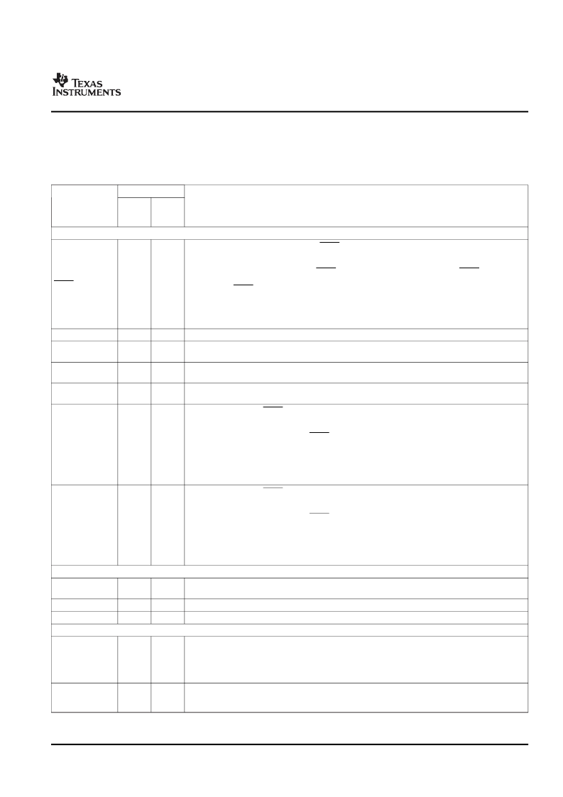
Table 2-3
describes the signals on the 280x devices. All digital inputs are TTL-compatible. All outputs are
3.3 V with CMOS levels. Inputs are not 5-V tolerant.
Table 2-3. Signal Descriptions
PIN NO.
GGM/
ZGM
BALL #
NAME
DESCRIPTION
(1)
PZ
PIN #
JTAG
JTAG test reset with internal pulldown. TRST, when driven high, gives the scan system control of
the operations of the device. If this signal is not connected or driven low, the device operates in its
functional mode, and the test reset signals are ignored.
NOTE: Do not use pullup resistors on TRST; it has an internal pull-down device. TRST is an active
high test pin and must be maintained low at all times during normal device operation. In a low-noise
environment, TRST may be left floating. In other instances, an external pulldown resistor is
highly
recommended
. The value of this resistor should be based on drive strength of the debugger pods
applicable to the design. A 2.2-k
resistor generally offers adequate protection. Since this is
application-specific, it is recommended that each target board be validated for proper operation of
the debugger and the application. (I,
↓
)
JTAG test clock with internal pullup (I,
↑
)
JTAG test-mode select (TMS) with internal pullup. This serial control input is clocked into the TAP
controller on the rising edge of TCK. (I,
↑
)
JTAG test data input (TDI) with internal pullup. TDI is clocked into the selected register (instruction
or data) on a rising edge of TCK. (I,
↑
)
JTAG scan out, test data output (TDO). The contents of the selected register (instruction or data)
are shifted out of TDO on the falling edge of TCK. (O/Z 8 mA drive)
Emulator pin 0. When TRST is driven high, this pin is used as an interrupt to or from the emulator
system and is defined as input/output through the JTAG scan. This pin is also used to put the
device into boundary-scan mode. With the EMU0 pin at a logic-high state and the EMU1 pin at a
logic-low state, a rising edge on the TRST pin would latch the device into boundary-scan mode.
(I/O/Z, 8 mA drive
↑
)
NOTE:
An external pullup resistor is recommended on this pin. The value of this resistor should be
based on the drive strength of the debugger pods applicable to the design. A 2.2-k
to 4.7-k
resistor is generally adequate. Since this is application-specific, it is recommended that each target
board be validated for proper operation of the debugger and the application.
Emulator pin 1. When TRST is driven high, this pin is used as an interrupt to or from the emulator
system and is defined as input/output through the JTAG scan. This pin is also used to put the
device into boundary-scan mode. With the EMU0 pin at a logic-high state and the EMU1 pin at a
logic-low state, a rising edge on the TRST pin would latch the device into boundary-scan mode.
(I/O/Z, 8 mA drive
↑
)
NOTE:
An external pullup resistor is recommended on this pin. The value of this resistor should be
based on the drive strength of the debugger pods applicable to the design. A 2.2-k
to 4.7-k
resistor is generally adequate. Since this is application-specific, it is recommended that each target
board be validated for proper operation of the debugger and the application.
FLASH
3.3-V Flash Core Power Pin. This pin should be connected to 3.3 V at all times. On the ROM
parts (C280x), this pin should be connected to V
DDIO
.
Test Pin. Reserved for TI. Must be left unconnected. (I/O)
Test Pin. Reserved for TI. Must be left unconnected. (I/O)
CLOCK
Output clock derived from SYSCLKOUT. XCLKOUT is either the same frequency, one-half the
frequency, or one-fourth the frequency of SYSCLKOUT. This is controlled by the bits 1, 0
(XCLKOUTDIV) in the XCLK register. At reset, XCLKOUT = SYSCLKOUT/4. The XCLKOUT signal
can be turned off by setting XCLKOUTDIV to 3. Unlike other GPIO pins, the XCLKOUT pin is not
placed in high-impedance state during a reset. (O/Z, 8 mA drive).
External Oscillator Input. This pin is to feed a clock from an external 3.3-V oscillator. In this case,
the X1 pin must be tied to GND. If a crystal/resonator is used (or if an external 1.8-V oscillator is
used to feed clock to X1 pin), this pin must be tied to GND. (I)
TRST
84
A6
TCK
75
A10
TMS
74
B10
TDI
73
C9
TDO
76
B9
EMU0
80
A8
EMU1
81
B7
V
DD3VFL
96
C4
TEST1
TEST2
97
98
A3
B3
XCLKOUT
66
E8
XCLKIN
90
B5
(1)
I = Input, O = Output, Z = High impedance, OD = Open drain,
↑
= Pullup,
↓
= Pulldown
Submit Documentation Feedback
Introduction
21
相關(guān)PDF資料 |
PDF描述 |
|---|---|
| TMS320F2809_07 | Digital Signal Processors |
| TMS320F28335_1 | Variable Capacitance Diode for TV Tuner VHF Tuning; Ratings VR (V): 32; Characteristics n: 12.0 min; Characteristics rs (ohm) max: 0.85; Characteristics C (pF) max: C2 = 32.2 to 37.5 C25 = 2.57 to 3.0; Characteristics CVR/CVR: 2/25; Cl: 2.777; Package: UFP |
| TMS4024 | 9 X 64 DIGITAL STORAGE BUFFER (FIFO) |
| TMS4024JC | 9 X 64 DIGITAL STORAGE BUFFER (FIFO) |
| TMS4024NC | 9 X 64 DIGITAL STORAGE BUFFER (FIFO) |
相關(guān)代理商/技術(shù)參數(shù) |
參數(shù)描述 |
|---|---|
| TMS320F2801ZGMA | 功能描述:數(shù)字信號(hào)處理器和控制器 - DSP, DSC 32-Bit Digital Sig Controller w/Flash RoHS:否 制造商:Microchip Technology 核心:dsPIC 數(shù)據(jù)總線寬度:16 bit 程序存儲(chǔ)器大小:16 KB 數(shù)據(jù) RAM 大小:2 KB 最大時(shí)鐘頻率:40 MHz 可編程輸入/輸出端數(shù)量:35 定時(shí)器數(shù)量:3 設(shè)備每秒兆指令數(shù):50 MIPs 工作電源電壓:3.3 V 最大工作溫度:+ 85 C 封裝 / 箱體:TQFP-44 安裝風(fēng)格:SMD/SMT |
| TMS320F2801ZGMS | 功能描述:數(shù)字信號(hào)處理器和控制器 - DSP, DSC 32-Bit Digital Sig Controller w/Flash RoHS:否 制造商:Microchip Technology 核心:dsPIC 數(shù)據(jù)總線寬度:16 bit 程序存儲(chǔ)器大小:16 KB 數(shù)據(jù) RAM 大小:2 KB 最大時(shí)鐘頻率:40 MHz 可編程輸入/輸出端數(shù)量:35 定時(shí)器數(shù)量:3 設(shè)備每秒兆指令數(shù):50 MIPs 工作電源電壓:3.3 V 最大工作溫度:+ 85 C 封裝 / 箱體:TQFP-44 安裝風(fēng)格:SMD/SMT |
| TMS320F280200DAS | 功能描述:32位微控制器 - MCU Piccolo Micro controller RoHS:否 制造商:Texas Instruments 核心:C28x 處理器系列:TMS320F28x 數(shù)據(jù)總線寬度:32 bit 最大時(shí)鐘頻率:90 MHz 程序存儲(chǔ)器大小:64 KB 數(shù)據(jù) RAM 大小:26 KB 片上 ADC:Yes 工作電源電壓:2.97 V to 3.63 V 工作溫度范圍:- 40 C to + 105 C 封裝 / 箱體:LQFP-80 安裝風(fēng)格:SMD/SMT |
| TMS320F280200DAT | 功能描述:32位微控制器 - MCU Piccolo Micro controller RoHS:否 制造商:Texas Instruments 核心:C28x 處理器系列:TMS320F28x 數(shù)據(jù)總線寬度:32 bit 最大時(shí)鐘頻率:90 MHz 程序存儲(chǔ)器大小:64 KB 數(shù)據(jù) RAM 大小:26 KB 片上 ADC:Yes 工作電源電壓:2.97 V to 3.63 V 工作溫度范圍:- 40 C to + 105 C 封裝 / 箱體:LQFP-80 安裝風(fēng)格:SMD/SMT |
| TMS320F280200PTS | 功能描述:32位微控制器 - MCU Piccolo Micro controller RoHS:否 制造商:Texas Instruments 核心:C28x 處理器系列:TMS320F28x 數(shù)據(jù)總線寬度:32 bit 最大時(shí)鐘頻率:90 MHz 程序存儲(chǔ)器大小:64 KB 數(shù)據(jù) RAM 大小:26 KB 片上 ADC:Yes 工作電源電壓:2.97 V to 3.63 V 工作溫度范圍:- 40 C to + 105 C 封裝 / 箱體:LQFP-80 安裝風(fēng)格:SMD/SMT |
發(fā)布緊急采購,3分鐘左右您將得到回復(fù)。