- 您現(xiàn)在的位置:買賣IC網(wǎng) > PDF目錄384019 > TMS27C020-25JE (Texas Instruments, Inc.) READ-ONLY MEMORIES PDF資料下載
參數(shù)資料
| 型號(hào): | TMS27C020-25JE |
| 廠商: | Texas Instruments, Inc. |
| 英文描述: | READ-ONLY MEMORIES |
| 中文描述: | 只讀存儲(chǔ)器 |
| 文件頁(yè)數(shù): | 7/15頁(yè) |
| 文件大?。?/td> | 206K |
| 代理商: | TMS27C020-25JE |
第1頁(yè)第2頁(yè)第3頁(yè)第4頁(yè)第5頁(yè)第6頁(yè)當(dāng)前第7頁(yè)第8頁(yè)第9頁(yè)第10頁(yè)第11頁(yè)第12頁(yè)第13頁(yè)第14頁(yè)第15頁(yè)
TMS27C020 262144 BY 8-BIT UV ERASABLE
TMS27PC020 262144 BY 8-BIT
PROGRAMMABLE READ-ONLY MEMORIES
SMLS020C – NOVEMBER 1990 – REVISED SEPTEMBER 1997
7
POST OFFICE BOX 1443
HOUSTON, TEXAS 77251–1443
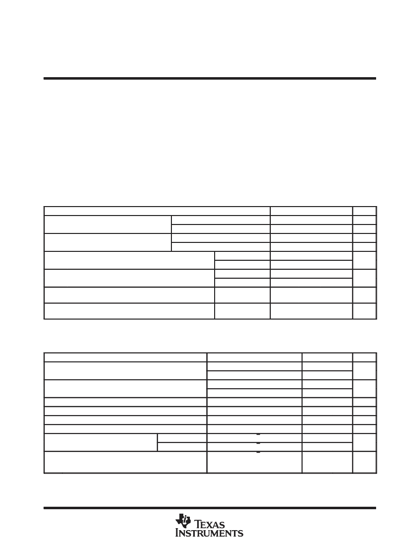
absolute maximum ratings over operating free-air temperature range (unless otherwise noted)
Supply voltage range, V
CC
(see Note 1) :
. . . . . . . . . . . . . . . . . . . . . . . . . . . . . . . . . . . . . . . . . . . . . .
Supply voltage range, V
PP
:
. . . . . . . . . . . . . . . . . . . . . . . . . . . . . . . . . . . . . . . . . . . . . . . . . . . . . . . .
Input voltage range (see Note 1), All inputs except A9 :
A9 :
. . . . . . . . . . . . . . . . . . . . . . . . . . . . . . . . . . . . . . . . . . . . . .
Output voltage range, with respect to V
SS
(see Note 1) :
Operating free-air temperature range (’27C020-_ _ JL, ’27PC020_ _FML) :
Operating free-air temperature range (’27C020-_ _JE, ’27PC020-_ _FME) :
Storage temperature range, T
stg
:
. . . . . . . . . . . . . . . . . . . . . . . . . . . . . . . . . . . . . . . . . . . . . . . . . .
Stresses beyond those listed under “absolute maximum ratings” may cause permanent damage to the device. These are stress ratings only, and
functional operation of the device at these or any other conditions beyond those indicated under “recommended operating conditions” is not
implied. Exposure to absolute-maximum-rated conditions for extended periods may affect device reliability.
NOTE 1: All voltage values are with respect to GND.
–0.6 V to 7 V
–0.6 V to 14 V
–0.6 V to V
CC
+ 1 V
–0.6 V to 13.5 V
–0.6 V to V
CC
+ 1 V
0
°
C to 70
°
C
– 40
°
C to 85
°
C
–65
°
C to 150
°
C
. . . . . . . . . . . . . . . . . . . . . . . . . . . .
. . . . . . . . . . . . . . . . . . . . . . . . . .
. . . . . . . . . . . . . . . . .
. . . . . . . . . . . . . . .
recommended operating conditions
MIN
4.5
NOM
MAX
5.5
UNIT
V
VCC
Supply voltage
Read mode (see Note 2)
5
SNAP! Pulse programming algorithm
6.25
6.5
6.75
V
VPP
Supply voltage
Read mode
VCC–0.6
12.75
VCC
13
VCC+0.6
13.25
V
SNAP! Pulse programming algorithm
V
VIH
High level dc input voltage
High-level dc input voltage
TTL
2
VCC+0.5
VCC+0.5
0.8
V
CMOS
VCC–0.2
–0.5
VIL
Low level dc input voltage
Low-level dc input voltage
TTL
V
CMOS
–0.5
GND+0.2
TA
Operating free-air temperature
’27C020-_ _JL,
’27PC020-_ _FML
0
70
°
C
TA
Operating free-air temperature
’27C020-_ _JE,
’27PC020-_ _FME
– 40
85
°
C
NOTE 2: VCC must be applied before or at the same time as VPP and removed after or at the same time as VPP. The device must not be
inserted into or removed from the board when VPP or VCC is applied.
electrical characteristics over full ranges of operating conditions
PARAMETER
TEST CONDITIONS
IOH = –20
μ
A
IOH = – 2 mA
IOL = 2.1 mA
IOL = 20
μ
A
VI = 0 V to 5.5 V
VO = 0 V to VCC
VPP = VCC = 5.5 V
VPP = 13 V
VCC = 5.5 V,
VCC = 5.5 V,
VCC = 5.5 V,
tcycle = minimum cycle time,
outputs open
MIN
MAX
UNIT
VOH
High level dc output voltage
High-level dc output voltage
VCC– 0.2
2.4
V
VOL
Low level dc output voltage
Low-level dc output voltage
0.4
V
0.1
±
1
±
1
10
II
IO
IPP1
IPP2
Input current (leakage)
μ
A
μ
A
μ
A
mA
Output current (leakage)
VPP supply current
VPP supply current (during program pulse)
50
ICC1
VCCsupply current (standby)
VCC supply current (standby)
TTL-input level
E = VIH
E = VCC
±
0.2 V
E = VIL
. . .
500
μ
A
CMOS-input level
100
ICC2
VCC supply current (active)
30
mA
Minimum cycle time = maximum access time.
相關(guān)PDF資料 |
PDF描述 |
|---|---|
| TMS27C020-25JL | READ-ONLY MEMORIES |
| TMS27PC020-10FME | READ-ONLY MEMORIES |
| TMS27C020-10FME | READ-ONLY MEMORIES |
| TMS27C020-10FML | READ-ONLY MEMORIES |
| TMS27C020-10JE | READ-ONLY MEMORIES |
相關(guān)代理商/技術(shù)參數(shù) |
參數(shù)描述 |
|---|---|
| TMS27C020-25JE4 | 制造商:未知廠家 制造商全稱:未知廠家 功能描述:x8 EPROM |
| TMS27C020-25JL | 制造商:TI 制造商全稱:Texas Instruments 功能描述:READ-ONLY MEMORIES |
| TMS27C020-25JL4 | 制造商:未知廠家 制造商全稱:未知廠家 功能描述:x8 EPROM |
| TMS27C040 | 制造商:TI 制造商全稱:Texas Instruments 功能描述:READ-ONLY MEMORIES |
| TMS27C128 | 制造商:TI 制造商全稱:Texas Instruments 功能描述:131 072-BIT UV ERASABLE PROGRAMMABLE READ-ONLY MEMORY |
發(fā)布緊急采購(gòu),3分鐘左右您將得到回復(fù)。