- 您現(xiàn)在的位置:買賣IC網(wǎng) > PDF目錄384019 > TMP320F28044ZGMQ (Texas Instruments, Inc.) Digital Signal Processor PDF資料下載
參數(shù)資料
| 型號: | TMP320F28044ZGMQ |
| 廠商: | Texas Instruments, Inc. |
| 元件分類: | 數(shù)字信號處理 |
| 英文描述: | Digital Signal Processor |
| 中文描述: | 數(shù)字信號處理器 |
| 文件頁數(shù): | 85/107頁 |
| 文件大小: | 784K |
| 代理商: | TMP320F28044ZGMQ |
第1頁第2頁第3頁第4頁第5頁第6頁第7頁第8頁第9頁第10頁第11頁第12頁第13頁第14頁第15頁第16頁第17頁第18頁第19頁第20頁第21頁第22頁第23頁第24頁第25頁第26頁第27頁第28頁第29頁第30頁第31頁第32頁第33頁第34頁第35頁第36頁第37頁第38頁第39頁第40頁第41頁第42頁第43頁第44頁第45頁第46頁第47頁第48頁第49頁第50頁第51頁第52頁第53頁第54頁第55頁第56頁第57頁第58頁第59頁第60頁第61頁第62頁第63頁第64頁第65頁第66頁第67頁第68頁第69頁第70頁第71頁第72頁第73頁第74頁第75頁第76頁第77頁第78頁第79頁第80頁第81頁第82頁第83頁第84頁當前第85頁第86頁第87頁第88頁第89頁第90頁第91頁第92頁第93頁第94頁第95頁第96頁第97頁第98頁第99頁第100頁第101頁第102頁第103頁第104頁第105頁第106頁第107頁
www.ti.com
WAKE INT
(A)
XCLKOUT
Address/Data
(internal)
t
d(WAKEIDLE)
t
w(WAKEINT)
TMS320F28044
Digital Signal Processor
SPRS357B–AUGUST 2006–REVISED MAY 2007
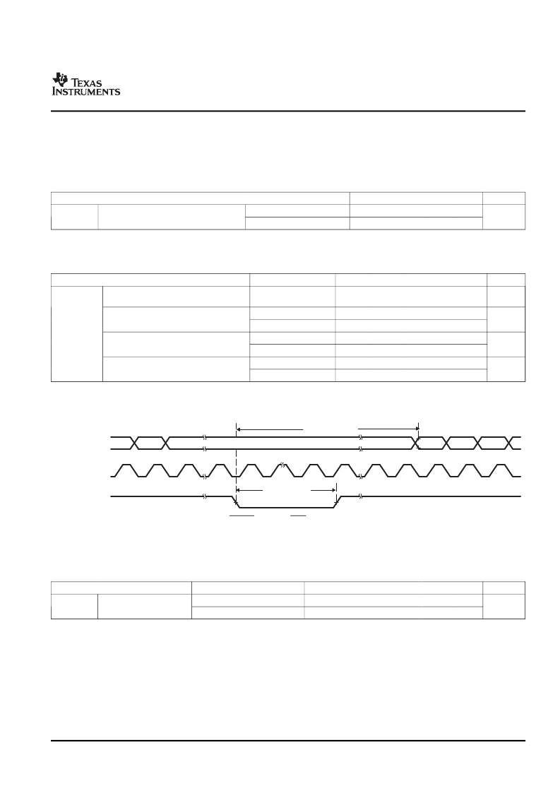
6.9.4
Low-Power Mode Wakeup Timing
Table 6-12
shows the timing requirements,
Table 6-13
shows the switching characteristics, and
Figure 6-10
shows the timing diagram for IDLE mode.
Table 6-12. IDLE Mode Timing Requirements
(1)
MIN
NOM
MAX
UNIT
Without input qualifier
With input qualifier
2t
c(SCO)
5t
c(SCO)
+ t
w(IQSW)
t
w(WAKE-INT)
Pulse duration, external wake-up signal
cycles
(1)
For an explanation of the input qualifier parameters, see
Table 6-11
.
Table 6-13. IDLE Mode Switching Characteristics
(1)
PARAMETER
Delay time, external wake signal to
program execution resume
(2)
TEST CONDITIONS
MIN
TYP
MAX
UNIT
Without input qualifier
With input qualifier
Without input qualifier
With input qualifier
Without input qualifier
With input qualifier
20t
c(SCO)
cycles
Wake-up from Flash
–
Flash module in active state
20t
c(SCO)
+ t
w(IQSW)
1050t
c(SCO)
1050t
c(SCO)
+ t
w(IQSW)
t
d(WAKE-IDLE)
cycles
Wake-up from Flash
–
Flash module in sleep state
20t
c(SCO)
cycles
Wake-up from SARAM
20t
c(SCO)
+ t
w(IQSW)
(1)
(2)
For an explanation of the input qualifier parameters, see
Table 6-11
.
This is the time taken to begin execution of the instruction that immediately follows the IDLE instruction. execution of an ISR (triggered
by the wake up) signal involves additional latency.
A.
WAKE INT can be any enabled interrupt, WDINT, XNMI, or XRS.
Figure 6-10. IDLE Entry and Exit Timing
Table 6-14. STANDBY Mode Timing Requirements
TEST CONDITIONS
Without input qualification
With input qualification
(1)
MIN
NOM
MAX
UNIT
3t
c(OSCCLK)
Pulse duration, external
wake-up signal
t
w(WAKE-INT)
cycles
(2 + QUALSTDBY) * t
c(OSCCLK)
(1)
QUALSTDBY is a 6-bit field in the LPMCR0 register.
Submit Documentation Feedback
Electrical Specifications
85
相關(guān)PDF資料 |
PDF描述 |
|---|---|
| TMP320F28044ZGMS | Digital Signal Processor |
| TMS320F28044_07 | Digital Signal Processor |
| TMS320F28044ZGMA | Digital Signal Processor |
| TMS320F28044ZGMQ | Digital Signal Processor |
| TMS320F28044ZGMS | Digital Signal Processor |
相關(guān)代理商/技術(shù)參數(shù) |
參數(shù)描述 |
|---|---|
| TMP320F28044ZGMS | 制造商:TI 制造商全稱:Texas Instruments 功能描述:Digital Signal Processor |
| TMP320F2810GHHA | 制造商:TI 制造商全稱:Texas Instruments 功能描述:DIGITAL SIGNAL PROCESSORS |
| TMP320F2810GHHMEP | 制造商:TI 制造商全稱:Texas Instruments 功能描述:Digital Signal Processors |
| TMP320F2810GHHS | 制造商:TI 制造商全稱:Texas Instruments 功能描述:DIGITAL SIGNAL PROCESSORS |
| TMP320F2810PBKA | 制造商:Texas Instruments 功能描述: |
發(fā)布緊急采購,3分鐘左右您將得到回復。