- 您現(xiàn)在的位置:買賣IC網(wǎng) > PDF目錄98266 > TMDS361PAG (TEXAS INSTRUMENTS INC) SPECIALTY CONSUMER CIRCUIT, PQFP64 PDF資料下載
參數(shù)資料
| 型號(hào): | TMDS361PAG |
| 廠商: | TEXAS INSTRUMENTS INC |
| 元件分類: | 消費(fèi)家電 |
| 英文描述: | SPECIALTY CONSUMER CIRCUIT, PQFP64 |
| 封裝: | PLASTIC, TQFP-64 |
| 文件頁數(shù): | 42/43頁 |
| 文件大?。?/td> | 2159K |
| 代理商: | TMDS361PAG |
第1頁第2頁第3頁第4頁第5頁第6頁第7頁第8頁第9頁第10頁第11頁第12頁第13頁第14頁第15頁第16頁第17頁第18頁第19頁第20頁第21頁第22頁第23頁第24頁第25頁第26頁第27頁第28頁第29頁第30頁第31頁第32頁第33頁第34頁第35頁第36頁第37頁第38頁第39頁第40頁第41頁當(dāng)前第42頁第43頁
ABSOLUTE MAXIMUM RATINGS
SLLS919A – DECEMBER 2008 – REVISED JANUARY 2009............................................................................................................................................ www.ti.com
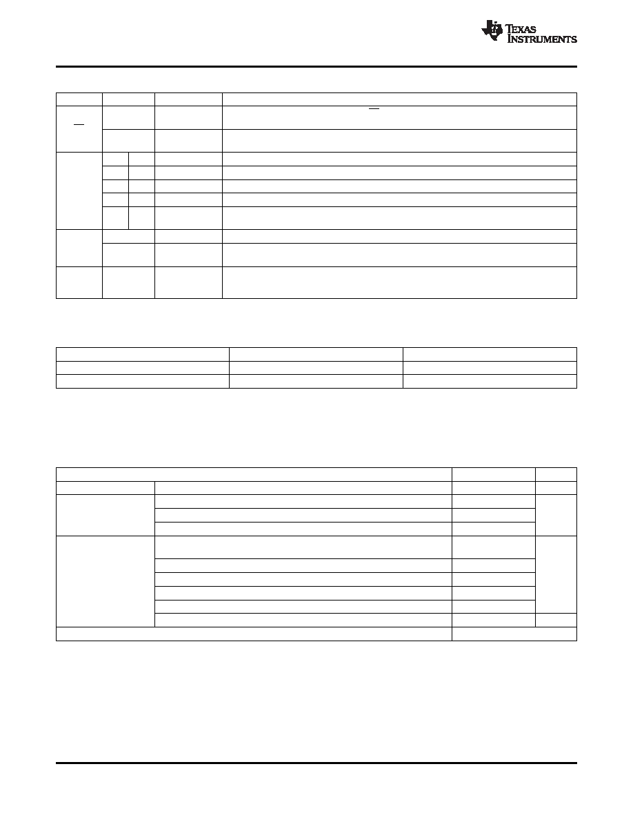
Table 2. Control-Pin Lookup Table(1)
SIGNAL
LEVEL
STATE
DESCRIPTION
Normal operational mode for device. If LP is left floating, then a weak internal pullup to VCC
H
Normal mode
pulls it to VCC.
LP
Low-power
Device is forced into a low-power state, causing the inputs and outputs to go to a
L
mode
high-impedance state. All other inputs are ignored.
S2
S1
H
Port 1
Port 1 is selected as the active port; all other ports are low.
S[2:1]
H
L
Port 2
Port 2 is selected as the active port; all other ports are low.
GPIO
L
Port 3
Port 3 is selected as the active port; all other ports are low.
mode
HPD[1:3] follow
L
H
Standby mode: HPD[1:3] follow HPD_sink.
HPD_SINK
L
I2C
Device is configured by I2C logic.
I2C_SEL
Device is configured by GPIO. If the I2C_SEL pin is left floating, then a weak internal pullup to
H
GPIO
VCC pulls the I2C_SEL pin high.
Driver output voltage swing precision control to aid with system compliance. The VSadj
Compliant
VSadj
4.02 k
resistor value can be selected to be 4.02 k
±10% based on the system requirement to pass
voltage
HDMI compliance.
(1)
(H) Logic high; (L) Logic low
ORDERING INFORMATION(1)
PART NUMBER
PART MARKING
PACKAGE
TMDS361PAGR
TMDS361
64-pin TQFP reel (large)
TMDS361PAG
TMDS361
64-pin TQFP tray
(1)
For the most current package and ordering information, see the Package Option Addendum at the end of this document, or see the TI
Web site at www.ti.com.
over operating free-air temperature range (unless otherwise noted)
(1)
VALUE
UNIT
Supply voltage range(2)
VCC
–0.3 to 3.6
V
TMDS I/O
–0.3 to 4
Voltage range
HPD and DDC I/O
–0.3 to 5.5
V
Control and status I/O
–0.3 to 5.5
Human body model(3) on SCL[1:3], SDA[1:3], HPD[1:3], D[0:2]+_[1:3],
±10,000
D[0:2]–_[1:3], CLK+_[1:3], CLK–_[1:3] pins
Human body model(3) on all other pins
±9,000
V
Charged-device model(4)
±1500
Electrostatic discharge
Machine model(5)
±200
IEC 61000-4-2(6), contact discharge
±8,000
IEC 61000-4-2(6), air discharge
±15,000
Continuous power dissipation
See Dissipation Ratings table
(1)
Stresses beyond those listed under Absolute Maximum Ratings may cause permanent damage to the device. These are stress ratings
only, and functional operation of the device at these or any other conditions beyond those indicated under Recommended Operating
Conditions is not implied. Exposure to absolute-maximum-rated conditions for extended periods may affect device reliability.
(2)
All voltage values, except differential voltages, are with respect to network ground terminal.
(3)
Tested in accordance with JEDEC Standard 22, Test Method A114-B
(4)
Tested in accordance with JEDEC Standard 22, Test Method C101-A
(5)
Tested in accordance with JEDEC Standard 22, Test Method A115-A
(6)
Tested in accordance with IEC EN 61000-4-2
8
Copyright 2008–2009, Texas Instruments Incorporated
Product Folder Link(s) :TMDS361
相關(guān)PDF資料 |
PDF描述 |
|---|---|
| TMDS442PNPG4 | SPECIALTY CONSUMER CIRCUIT, PQFP128 |
| TMDS442PNPR | SPECIALTY CONSUMER CIRCUIT, PQFP128 |
| TMDS442PNP | SPECIALTY CONSUMER CIRCUIT, PQFP128 |
| TMDS442PNPRG4 | SPECIALTY CONSUMER CIRCUIT, PQFP128 |
| TMDS461PZIT | SPECIALTY CONSUMER CIRCUIT, PQFP100 |
相關(guān)代理商/技術(shù)參數(shù) |
參數(shù)描述 |
|---|---|
| TMDS361PAGR | 功能描述:視頻開關(guān) IC 3 to 1 HDMI Switch RoHS:否 制造商:Texas Instruments 開關(guān)數(shù)量:4 開啟電阻(最大值):12 Ohms 傳播延遲時(shí)間: 開啟時(shí)間(最大值): 關(guān)閉時(shí)間(最大值): 最大工作溫度:+ 85 C 最小工作溫度:- 40 C 封裝 / 箱體:WQFN-42 封裝:Reel |
| TMDS361PAGT | 制造商:TI 制造商全稱:Texas Instruments 功能描述:1080p - Deep Color 3-to-1 HDMI/DVI Switch with Adaptive Equalization |
| TMDS37000 | 制造商:Texas Instruments 功能描述:STARTER PACK TMS370 |
| TMDS3700572A | 制造商:TI 制造商全稱:Texas Instruments 功能描述:TMS370 MICROCONTROLLER FAMILY DATA BOOK |
| TMDS3740555-09 | 功能描述:開發(fā)軟件 TMS370 Optimizing C Cross Compiler RoHS:否 制造商:Atollic Inc. 產(chǎn)品:Compilers/Debuggers 用于:ARM7, ARM9, Cortex-A, Cortex-M, Cortex-R Processors |
發(fā)布緊急采購,3分鐘左右您將得到回復(fù)。