- 您現(xiàn)在的位置:買賣IC網(wǎng) > PDF目錄384008 > TLV2211Y (Texas Instruments, Inc.) Advanced LinCMOSE RAIL-TO-RAIL MICROPOWER SINGLE OPERATIONAL AMPLIFIERS PDF資料下載
參數(shù)資料
| 型號: | TLV2211Y |
| 廠商: | Texas Instruments, Inc. |
| 英文描述: | Advanced LinCMOSE RAIL-TO-RAIL MICROPOWER SINGLE OPERATIONAL AMPLIFIERS |
| 中文描述: | 高級LinCMOSE軌至軌微功耗單運算放大器 |
| 文件頁數(shù): | 5/29頁 |
| 文件大小: | 529K |
| 代理商: | TLV2211Y |
第1頁第2頁第3頁第4頁當前第5頁第6頁第7頁第8頁第9頁第10頁第11頁第12頁第13頁第14頁第15頁第16頁第17頁第18頁第19頁第20頁第21頁第22頁第23頁第24頁第25頁第26頁第27頁第28頁第29頁
TLV2211, TLV2211Y
Advanced LinCMOS
RAIL-TO-RAIL
MICROPOWER SINGLE OPERATIONAL AMPLIFIERS
SLOS156B – MAY 1996 – REVISED JANUARY 1997
5
POST OFFICE BOX 655303
DALLAS, TEXAS 75265
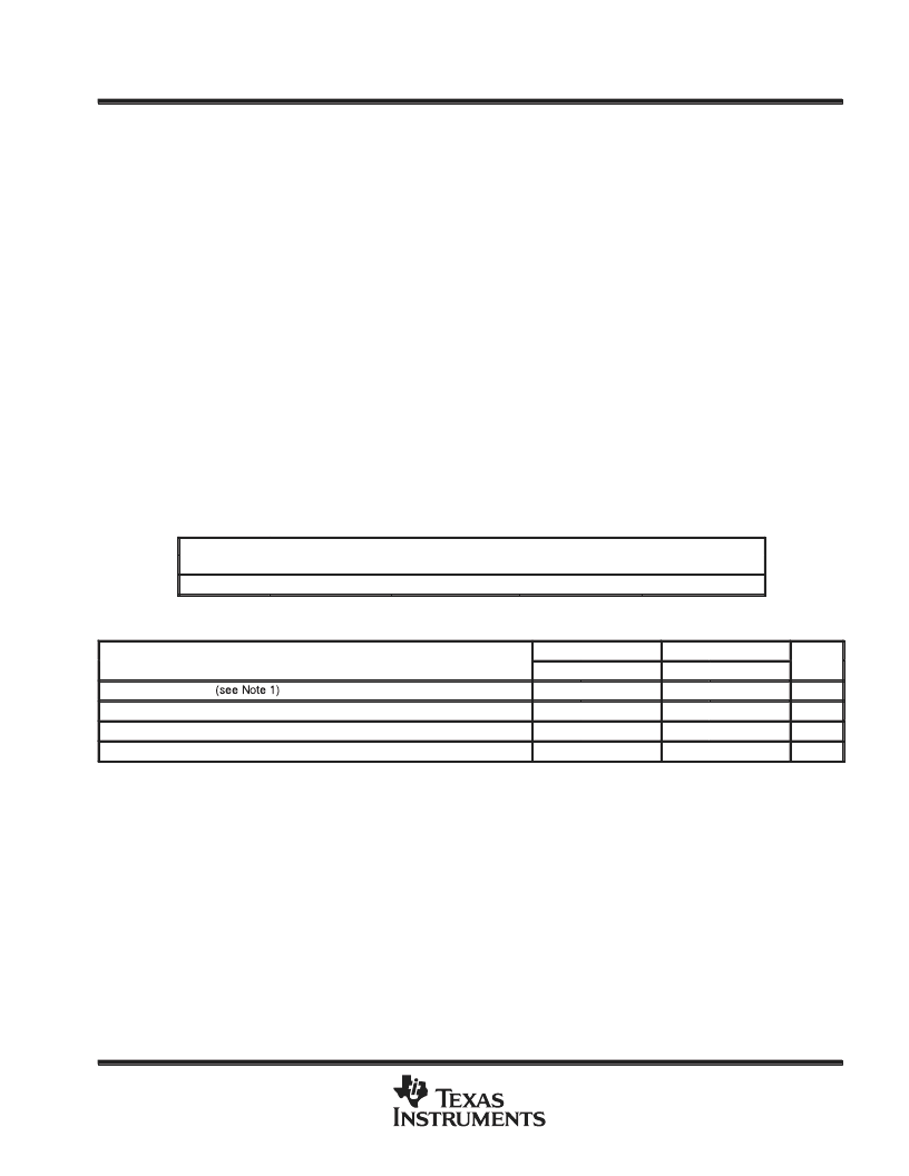
absolute maximum ratings over operating free-air temperature range (unless otherwise noted)
Supply voltage, V
DD
(see Note 1)
Differential input voltage, V
ID
(see Note 2)
Input voltage range, V
I
(any input, see Note 1)
Input current, I
I
(each input)
Output current, I
O
. . . . . . . . . . . . . . . . . . . . . . . . . . . . . . . . . . . . . . . . . . . . . . . . . . . . . . . . . . . . . . . . . . . . . . .
Total current into V
DD+
. . . . . . . . . . . . . . . . . . . . . . . . . . . . . . . . . . . . . . . . . . . . . . . . . . . . . . . . . . . . . . . . . .
Total current out of V
DD–
. . . . . . . . . . . . . . . . . . . . . . . . . . . . . . . . . . . . . . . . . . . . . . . . . . . . . . . . . . . . . . . .
Duration of short-circuit current (at or below) 25
°
C (see Note 3)
Continuous total power dissipation
. . . . . . . . . . . . . . . . . . . . . . . . . . . . . . . . . . . . .
Operating free-air temperature range, T
A
: TLV2211C
TLV2211I
Storage temperature range, T
stg
. . . . . . . . . . . . . . . . . . . . . . . . . . . . . . . . . . . . . . . . . . . . . . . . . . .
Lead temperature 1,6 mm (1/16 inch) from case for 10 seconds: DBV package
12 V
±
V
DD
. . . . . . . . . . . . . . . . . . . . . . . . . . . . . . . . . . . . . . . . . . . . . . . . . . . . . . . . . . . .
. . . . . . . . . . . . . . . . . . . . . . . . . . . . . . . . . . . . . . . . . . . . . . . . . . .
. . . . . . . . . . . . . . . . . . . . . . . . . . . . . . . . . . . . . . . .
. . . . . . . . . . . . . . . . . . . . . . . . . . . . . . . . . . . . . . . . . . . . . . . . . . . . . . . . . . . . . . .
–0.3 V to V
DD
±
5 mA
±
50 mA
±
50 mA
±
50 mA
unlimited
. . . . . . . . . . . . . . . . . . . . . . . . . . . . . .
See Dissipation Rating Table
. . . . . . . . . . . . . . . . . . . . . . . . . . . . . . . . . . .
. . . . . . . . . . . . . . . . . . . . . . . . . . . . . . . . . .
0
°
C to 70
°
C
–40
°
C to 85
°
C
–65
°
C to 150
°
C
260
°
C
. . . . . . . . . . . . . . . . . .
Stresses beyond those listed under “absolute maximum ratings” may cause permanent damage to the device. These are stress ratings only, and
functional operation of the device at these or any other conditions beyond those indicated under “recommended operating conditions” is not
implied. Exposure to absolute-maximum-rated conditions for extended periods may affect device reliability.
NOTES:
1. All voltage values, except differential voltages, are with respect to VDD –.
2. Differential voltages are at the noninverting input with respect to the inverting input. Excessive current flows when input is brought
below VDD– – 0.3 V.
3. The output may be shorted to either supply. Temperature and/or supply voltages must be limited to ensure that the maximum
dissipation rating is not exceeded.
DISSIPATION RATING TABLE
PACKAGE
TA
≤
25
°
C
POWER RATING
DERATING FACTOR
ABOVE TA = 25
°
C
1.2 mW/
°
C
TA = 70
°
C
POWER RATING
TA = 85
°
C
POWER RATING
DBV
150 mW
96 mW
78 mW
recommended operating conditions
TLV2211C
MIN
2.7
TLV2211I
MIN
2.7
UNIT
MAX
MAX
Supply voltage, VDD
Input voltage range, VI
Common-mode input voltage, VIC
Operating free-air temperature, TA
NOTE 1: All voltage values, except differential voltages, are with respect to VDD –.
10
10
V
VDD–
VDD–
VDD+ –1.3
VDD+ –1.3
70
VDD–
VDD–
–40
VDD+ –1.3
VDD+ –1.3
85
V
V
°
C
0
相關PDF資料 |
PDF描述 |
|---|---|
| TLV2221CDBV | Advanced LinCMOSE RAIL-TO-RAIL VERY LOW-POWER SINGLE OPERATIONAL AMPLIFIERS |
| TLV2221IDBV | Advanced LinCMOSE RAIL-TO-RAIL VERY LOW-POWER SINGLE OPERATIONAL AMPLIFIERS |
| TLV2221Y | Advanced LinCMOSE RAIL-TO-RAIL VERY LOW-POWER SINGLE OPERATIONAL AMPLIFIERS |
| TLV2231CDBV | Advanced LinCMOSE RAIL-TO-RAIL LOW-POWER SINGLE OPERATIONAL AMPLIFIERS |
| TLV2231IDBV | Advanced LinCMOSE RAIL-TO-RAIL LOW-POWER SINGLE OPERATIONAL AMPLIFIERS |
相關代理商/技術參數(shù) |
參數(shù)描述 |
|---|---|
| TLV2217 | 制造商:TI 制造商全稱:Texas Instruments 功能描述:LOW DROPOUT FIXED VOLTAGE REGULATORS |
| TLV2217_07 | 制造商:TI 制造商全稱:Texas Instruments 功能描述:LOW-DROPOUT FIXED-VOLTAGE REGULATOES |
| TLV2217-18 | 制造商:TI 制造商全稱:Texas Instruments 功能描述:LOW-DROPOUT FIXED-VOLTAGE REGULATOES |
| TLV2217-18KCS | 功能描述:低壓差穩(wěn)壓器 - LDO 1.8-V Fixed-Voltage RoHS:否 制造商:Texas Instruments 最大輸入電壓:36 V 輸出電壓:1.4 V to 20.5 V 回動電壓(最大值):307 mV 輸出電流:1 A 負載調節(jié):0.3 % 輸出端數(shù)量: 輸出類型:Fixed 最大工作溫度:+ 125 C 安裝風格:SMD/SMT 封裝 / 箱體:VQFN-20 |
| TLV2217-18KCSE3 | 功能描述:低壓差穩(wěn)壓器 - LDO 1.8-V Fixed-Voltage RoHS:否 制造商:Texas Instruments 最大輸入電壓:36 V 輸出電壓:1.4 V to 20.5 V 回動電壓(最大值):307 mV 輸出電流:1 A 負載調節(jié):0.3 % 輸出端數(shù)量: 輸出類型:Fixed 最大工作溫度:+ 125 C 安裝風格:SMD/SMT 封裝 / 箱體:VQFN-20 |
發(fā)布緊急采購,3分鐘左右您將得到回復。