- 您現(xiàn)在的位置:買賣IC網(wǎng) > PDF目錄384006 > TLE2161MJG (Texas Instruments, Inc.) EXCALIBUR JFET-INPUT HIGH-OUTPUT-DRIVE mPOWER OPERATIONAL AMPLIFIERS PDF資料下載
參數(shù)資料
| 型號(hào): | TLE2161MJG |
| 廠商: | Texas Instruments, Inc. |
| 英文描述: | EXCALIBUR JFET-INPUT HIGH-OUTPUT-DRIVE mPOWER OPERATIONAL AMPLIFIERS |
| 中文描述: | 神劍JFET輸入高輸出驅(qū)動(dòng)MPOWER的運(yùn)算放大器 |
| 文件頁(yè)數(shù): | 1/29頁(yè) |
| 文件大小: | 457K |
| 代理商: | TLE2161MJG |
當(dāng)前第1頁(yè)第2頁(yè)第3頁(yè)第4頁(yè)第5頁(yè)第6頁(yè)第7頁(yè)第8頁(yè)第9頁(yè)第10頁(yè)第11頁(yè)第12頁(yè)第13頁(yè)第14頁(yè)第15頁(yè)第16頁(yè)第17頁(yè)第18頁(yè)第19頁(yè)第20頁(yè)第21頁(yè)第22頁(yè)第23頁(yè)第24頁(yè)第25頁(yè)第26頁(yè)第27頁(yè)第28頁(yè)第29頁(yè)
TLE2161, TLE2161A, TLE2161B
EXCALIBUR JFET-INPUT HIGH-OUTPUT-DRIVE
μ
POWER OPERATIONAL AMPLIFIERS
SLOS049D – NOVEMBER 1989 – REVISED MAY 1996
1
POST OFFICE BOX 655303
DALLAS, TEXAS 75265
Excellent Output Drive Capability
V
O
=
±
2.5 V Min at R
L
= 100
,
V
CC
±
=
±
5 V
V
O
=
±
12.5 V Min at R
L
= 600
,
V
CC
±
=
±
15 V
Low Supply Current . . . 280
μ
A Typ
Decompensated for High Slew Rate and
Gain-Bandwidth Product
A
VD
= 0.5 Min
Slew Rate = 10 V/
μ
s Typ
Gain-Bandwidth Product = 6.5 MHz Typ
Wide Operating Supply Voltage Range
V
CC
±
=
±
3.5 V to
±
18 V
High Open-Loop Gain . . . 280 V/mV Typ
Low Offset Voltage . . . 500
μ
V Max
Low Offset Voltage Drift With Time
0.04
μ
V/Month Typ
Low Input Bias Current . . . 5 pA Typ
description
The TLE2161, TLE2161A, and TLE2161B are
JFET-input, low-power, precision operational
amplifiers manufactured using the Texas
Instruments Excalibur process. Decompensated
for stability with a minimum closed-loop gain of 5,
these devices combine outstanding output drive
capability with low power consumption, excellent
dc precision, and high gain-bandwidth product.
In addition to maintaining the traditional JFET
advantages of fast slew rates and low input bias
and offset currents, the Excalibur process offers
outstanding parametric stability over time and
temperature. This results in a device that remains
precise even with changes in temperature and
over years of use.
AVAILABLE OPTIONS
PACKAGE
TA
VIOmax
AT 25 C
SMALL
OUTLINE
(D)
CHIP
CARRIER
(FK)
CERAMIC
DIP
(JG)
PLASTIC
DIP
(P)
0
°
C
to
70
°
C
500
μ
V
1 5 mV
1.5 mV
3 mV
500
μ
V
1 5 mV
1.5 mV
3 mV
500
μ
V
1 5 mV
1.5 mV
3 mV
—
TLE2161ACD
TLE2161CD
—
—
TLE2161BCP
TLE2161ACP
TLE2161CP
—
—
–40
°
C
to
85
°
C
–55
°
C
to
125
°
C
—
TLE2161AID
TLE2161ID
—
—
TLE2161BIP
TLE2161AIP
TLE2161IP
—
—
—
TLE2161AMD
TLE2161MD
—
TLE2161AMFK
TLE2161MFK
TLE2161BMJG
TLE2161AMJG
TLE2161MJG
TLE2161BMP
TLE2161AMP
TLE2161MP
The D packages are available taped and reeled. Add R suffix to device type (e.g., TLE2161ACDR).
Please be aware that an important notice concerning availability, standard warranty, and use in critical applications of
Texas Instruments semiconductor products and disclaimers thereto appears at the end of this data sheet.
PRODUCTION DATA information is current as of publication date.
Products conform to specifications per the terms of Texas Instruments
standard warranty. Production processing does not necessarily include
testing of all parameters.
Copyright
1996, Texas Instruments Incorporated
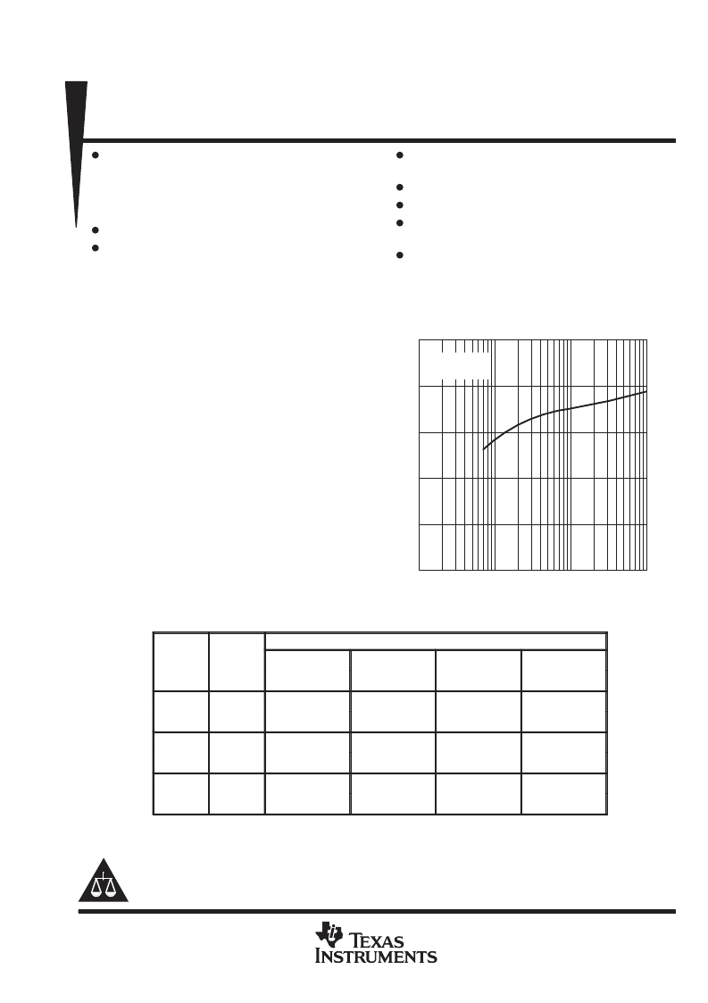
10 k
1 k
100
RL – Load Resistance –
10
0
2
4
6
8
10
TA = 25
°
C
MAXIMUM PEAK-TO-PEAK OUTPUT VOLTAGE
vs
LOAD RESISTANCE
–
VO
VCC
±
=
±
5 V
相關(guān)PDF資料 |
PDF描述 |
|---|---|
| TLE2161MD | EXCALIBUR JFET-INPUT HIGH-OUTPUT-DRIVE mPOWER OPERATIONAL AMPLIFIERS |
| TLE2161MFK | EXCALIBUR JFET-INPUT HIGH-OUTPUT-DRIVE mPOWER OPERATIONAL AMPLIFIERS |
| TLE2161AMD | EXCALIBUR JFET-INPUT HIGH-OUTPUT-DRIVE mPOWER OPERATIONAL AMPLIFIERS |
| TLE2161AMFK | EXCALIBUR JFET-INPUT HIGH-OUTPUT-DRIVE mPOWER OPERATIONAL AMPLIFIERS |
| TLE2161AMJG | EXCALIBUR JFET-INPUT HIGH-OUTPUT-DRIVE mPOWER OPERATIONAL AMPLIFIERS |
相關(guān)代理商/技術(shù)參數(shù) |
參數(shù)描述 |
|---|---|
| TLE2161MJGB | 制造商:Texas Instruments 功能描述:OP Amp Single GP 制造商:Rochester Electronics LLC 功能描述:- Bulk |
| TLE2161MLB | 制造商:Rochester Electronics LLC 功能描述:- Bulk |
| TLE2161MP | 制造商:Rochester Electronics LLC 功能描述:- Bulk |
| TLE2210 | 制造商:Philips Lumileds 功能描述:UV TUBE 22W CIRCULAR |
| TLE2227CDW | 制造商:Rochester Electronics LLC 功能描述:- Bulk |
發(fā)布緊急采購(gòu),3分鐘左右您將得到回復(fù)。