- 您現(xiàn)在的位置:買賣IC網(wǎng) > PDF目錄384002 > TL507C (Texas Instruments, Inc.) ANALOG-TO-DIGITAL CONVERTER PDF資料下載
參數(shù)資料
| 型號: | TL507C |
| 廠商: | Texas Instruments, Inc. |
| 英文描述: | ANALOG-TO-DIGITAL CONVERTER |
| 中文描述: | 模擬到數(shù)字轉(zhuǎn)換器 |
| 文件頁數(shù): | 6/8頁 |
| 文件大小: | 119K |
| 代理商: | TL507C |
TL507C, TL507l
ANALOG-TO-DIGITAL CONVERTER
SLAS041 – OCTOBER 1979 – REVISED OCTOBER 1988
6
POST OFFICE BOX 655303
DALLAS, TEXAS 75265
PRINCIPLES OF OPERATION
The TL507 is a single-slope analog-to-digital converter. All single-slope converters are basically voltage-to-time
or current-to-time converters. A study of the functional block diagram shows the versatility of the TL507.
An external clock signal is applied through a buffer to a negative-edge-triggered synchronous counter.
Binary-weighted resistors from the counter are connected to an operational amplifier used as an adder. The
operational amplifier generates a signal that ramps from 0.75
V
CC1
down to 0.25
V
CC1
. Comparator 1
compares the ramp signal to the analog input signal. Comparator 2 functions as a fault defector. With the analog
input voltage in the range 0.25
V
CC1
to 0.75
V
CC1
, the duty cycle of the output signal is determined by the
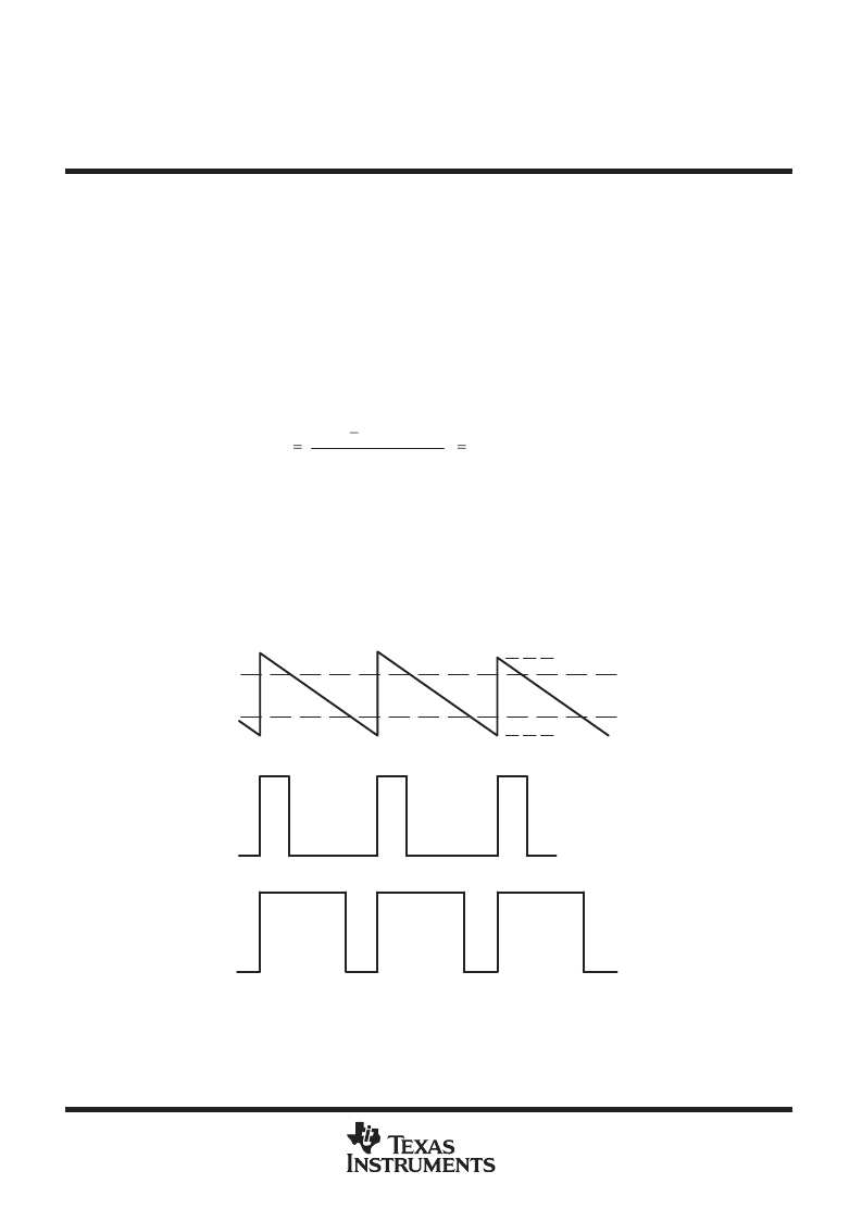
unknown analog input, as shown in Figure 2 and the Function Table.
For illustration, assume V
CC1
= 5.12 V,
0.25
V
CC1
= 1.28 V
(0.75
1 binary count
0.25) VCC1
128
20 mV
0.75
V
CC1
– 1 count = 3.82 V
The output is an open-collector n-p-n transistor capable of withstanding up to 18 V in the off state. The output
is current limited to the 8- to 12-mA range; however, care must be taken to ensure that the output does not
exceed 5.5 V in the on state.
The voltage regulator section allows operation f rom either an unregulated 8- to 18-V V
CC2
source or a regulated
3.5- to 6-V V
CC1
source. Regardless of which external power source is used, the internal circuitry operates at
V
CC1
. When operating from a V
CC1
source, V
CC2
may be connected to V
CC1
or left open. When operating from
a V
CC2
source, V
CC1
can be used as a reference voltage output.
Analog Input
Level 1
1.28 V
3.82 V
Output for
Input Level 2
Output for
Input Level 1
Ramp Input to
Comparator 1
Analog Input
Level 2
Figure 2
相關(guān)PDF資料 |
PDF描述 |
|---|---|
| TL750L05C | LOW-DROPOUT VOLTAGE REGULATORS |
| TL7702BMU | SUPPLY-VOLTAGE SUPERVISORS |
| TL7702BID | SUPPLY-VOLTAGE SUPERVISORS |
| TL7702BMFK | SUPPLY-VOLTAGE SUPERVISORS |
| TL7705BMFK | SUPPLY-VOLTAGE SUPERVISORS |
相關(guān)代理商/技術(shù)參數(shù) |
參數(shù)描述 |
|---|---|
| TL507CP | 制造商:TI 制造商全稱:Texas Instruments 功能描述:ANALOG-TO-DIGITAL CONVERTER |
| TL507L | 制造商:TI 制造商全稱:Texas Instruments 功能描述:ANALOG-TO-DIGITAL CONVERTER |
| TL50AQ | 制造商:Banner Engineering 功能描述:Tower Light, 50mm, Audiable Alarm, 18-30VDC/24VAC, Black, QDC, 11374 |
| TL50B | 制造商:Banner Engineering 功能描述:TL50B TOWER LIGHT |
| TL50BA | 制造商:Banner Engineering 功能描述:TL50BA TOWER LIGHT |
發(fā)布緊急采購,3分鐘左右您將得到回復(fù)。