- 您現(xiàn)在的位置:買賣IC網(wǎng) > PDF目錄383949 > TL16C550BI (Texas Instruments, Inc.) ASYNCHRONOUS COMMUNICATIONS ELEMENT PDF資料下載
參數(shù)資料
| 型號: | TL16C550BI |
| 廠商: | Texas Instruments, Inc. |
| 英文描述: | ASYNCHRONOUS COMMUNICATIONS ELEMENT |
| 中文描述: | 異步通信元 |
| 文件頁數(shù): | 20/35頁 |
| 文件大小: | 499K |
| 代理商: | TL16C550BI |
第1頁第2頁第3頁第4頁第5頁第6頁第7頁第8頁第9頁第10頁第11頁第12頁第13頁第14頁第15頁第16頁第17頁第18頁第19頁當(dāng)前第20頁第21頁第22頁第23頁第24頁第25頁第26頁第27頁第28頁第29頁第30頁第31頁第32頁第33頁第34頁第35頁
TL16C550B, TL16C550BI
ASYNCHRONOUS COMMUNICATIONS ELEMENT
SLLS136B – JANUARY 1994 – REVISED AUGUST 1996
20
POST OFFICE BOX 655303
DALLAS, TEXAS 75265
PRINCIPLES OF OPERATION
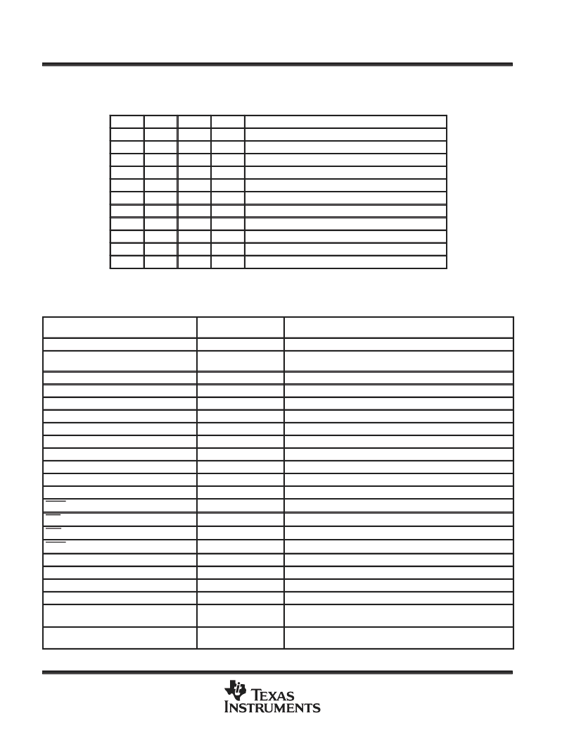
Table 1. Register Selection
DLAB
A2
A1
A0
REGISTER
0
L
L
L
Receiver buffer (read), transmitter holding (write)
0
L
L
H
Interrupt enable register
X
L
H
L
Interrupt identification register (read only)
X
L
H
L
FIFO control register (write)
X
L
H
H
Line control register
X
H
L
L
Modem control register
X
H
L
H
Line status register
X
H
H
L
Modem status register
X
H
H
H
Scratch register
1
L
L
L
Divisor latch (LSB)
1
L
L
H
Divisor latch (MSB)
The divisor latch access bit (DLAB) is the most significant bit of the line control register. The DLAB signal
is controlled by writing to this bit location (see Table 3).
Table 2. ACE Reset Functions
REGISTER/SIGNAL
RESET
CONTROL
RESET STATE
Interrupt Enable Register
Master Reset
All bits cleared (bits 0–3 forced and bits 4–7 permanent)
Interrupt Identification Register
Master Reset
Bit 0 is set, bits 1–3 are cleared, and bits 4–7 are permanently
cleared
FIFO Control Register
Master Reset
All bits cleared
Line Control Register
Master Reset
All bits cleared
Modem Control Register
Master Reset
All bits cleared (5–7 permanent)
Line Status Register
Master Reset
Bits 5 and 6 are set, all other bits are cleared
Modem Status Register
Master Reset
Bits 0–3 are cleared, bits 4–7 are input signals
SOUT
Master Reset
High
INTRPT (receiver error flag)
Read LSR/MR
Low
INTRPT (received data available)
Read RBR/MR
Low
INTRPT (transmitter holding register empty)
Read IR/Write THR/MR
Low
INTRPT (modem status changes)
Read MSR/MR
Low
OUT2
Master Reset
High
RTS
Master Reset
High
DTR
Master Reset
High
OUT1
Master Reset
High
Scratch Register
Master Reset
No effect
Divisor Latch (LSB and MSB) Registers
Master Reset
No effect
Receiver Buffer Registers
Master Reset
No effect
Transmitter Holding Registers
Master Reset
No effect
RCVR FIFO
MR/FCR1–FCR0/
FCR0
All bits low
XMIT FIFO
MR/FCR2–FCR0/
FCR0
All bits low
相關(guān)PDF資料 |
PDF描述 |
|---|---|
| TL16C550 | ASYNCHRONOUS COMMUNICATIONS ELEMENT |
| TL16C550BIN | ASYNCHRONOUS COMMUNICATIONS ELEMENT |
| TL16C550CIN | ASYNCHRONOUS COMMUNICATIONS ELEMENT WITH AUTOFLOW CONTROL |
| TL16C550CIPFB | ASYNCHRONOUS COMMUNICATIONS ELEMENT WITH AUTOFLOW CONTROL |
| TL16C552AMPN | DUAL ASYNCHRONOUS COMMUNICATIONS ELEMENT WITH FIFO |
相關(guān)代理商/技術(shù)參數(shù) |
參數(shù)描述 |
|---|---|
| TL16C550BIFN | 制造商:TI 制造商全稱:Texas Instruments 功能描述:ASYNCHRONOUS COMMUNICATIONS ELEMENT |
| TL16C550BIN | 制造商:TI 制造商全稱:Texas Instruments 功能描述:ASYNCHRONOUS COMMUNICATIONS ELEMENT |
| TL16C550BIPT | 制造商:TI 制造商全稱:Texas Instruments 功能描述:ASYNCHRONOUS COMMUNICATIONS ELEMENT |
| TL16C550BN | 制造商:Rochester Electronics LLC 功能描述:- Bulk |
| TL16C550BPT | 制造商:Rochester Electronics LLC 功能描述:- Tape and Reel |
發(fā)布緊急采購,3分鐘左右您將得到回復(fù)。