- 您現(xiàn)在的位置:買賣IC網(wǎng) > PDF目錄385927 > TL026C (Texas Instruments, Inc.) DIFFERENTIAL HIGH-FREQUENCY AMPLIFIER WITH AGC PDF資料下載
參數(shù)資料
| 型號(hào): | TL026C |
| 廠商: | Texas Instruments, Inc. |
| 英文描述: | DIFFERENTIAL HIGH-FREQUENCY AMPLIFIER WITH AGC |
| 中文描述: | 微分高頻率AGC放大器 |
| 文件頁數(shù): | 5/9頁 |
| 文件大小: | 135K |
| 代理商: | TL026C |
TL026C
DIFFERENTIAL HIGH-FREQUENCY AMPLIFIER WITH AGC
SLFS007A – JUNE 1985 – REVISED JULY 1990
5
POST OFFICE BOX 655303
DALLAS, TEXAS 75265
APPLICATION INFORMATION
gain characteristics
Figure 5 shows the differential voltage amplification versus the differential gain-control voltage (V
AGC
– V
ref
).
V
AGC
is the absolute voltage applied to the A
GC
input and V
ref
is the dc voltage at the REF OUT output. As V
AGC
increases with respect to V
ref
, the TL026C gain changes from maximum to minimum. As shown in Figure 5 for
example, V
AGC
would have to vary from approximately 180 mV less than V
ref
to approximately 180 mV greater
than V
ref
to change the gain from maximum to minimum. The total signal change in V
AGC
is defined by the
following equation.
V
AGC
= V
ref
+ 180 mV – (V
ref
– 180 mV)
V
AGC
= 360 mV
(1)
However, because V
AGC
varies as the ac AGC signal varies and also differentially around V
ref
, then V
AGC
should
have an ac signal component and a dc component. To preserve the dc and thermal tracking of the device, this
dc voltage must be generated from V
ref
. To apply proper bias to the AGC input, the external circuit used to
generate V
AGC
must combine these two voltages. Figures 6 and 7 show two circuits that will perform this
operation and are easy to implement. The circuits use a standard dual operational amplifier for AGC feedback.
By providing rectification and the required feedback gain, these circuits are also complete AGC systems.
circuit operation
Amplifier A1 amplifies and inverts the rectified and filtered AGC signal voltage V
C
producing output voltage V1.
Amplifier A2 is a differential amplifier that inverts V1 again and adds the scaled V
ref
voltage. This conditioning
makes V
AGC
the sum of the signal plus the scaled V
ref
. As the signal voltage increases, V
AGC
increases and
the gain of the TL026C is reduced. This maintains a constant output level.
feedback circuit equations
Following the AGC input signal (Figures 6 and 7) from the OUT output through the feedback amplifiers to the
AGC input produces the following equations:
(2)
1. AC ouput to diode D1, assuming sinusoidal signals
V
O
= V
OP
(sin (wt))
where:
V
OP
= peak voltage of V
O
(3)
2. Diode D1 and capacitor C1 output
V
C
= V
OP
– V
F
where:
VF = forward voltage drop of D1
V
C
= voltage across capacitor C1
(4)
3. A1 output
V1
R2
C
(5)
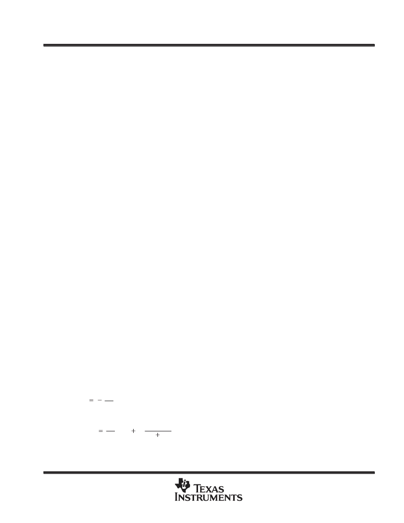
4. A2 output (R3 = R4)
V
AGC
R2
C
2
R6
R5
R6V
ref
相關(guān)PDF資料 |
PDF描述 |
|---|---|
| TL070CPW | JFET-INPUT OPERATIONAL AMPLIFIER |
| TL070D | JFET-INPUT OPERATIONAL AMPLIFIER |
| TL070ID | JFET-INPUT OPERATIONAL AMPLIFIER |
| TL070MD | JFET-INPUT OPERATIONAL AMPLIFIER |
| TL070MP | JFET-INPUT OPERATIONAL AMPLIFIER |
相關(guān)代理商/技術(shù)參數(shù) |
參數(shù)描述 |
|---|---|
| TL026CD | 功能描述:視頻放大器 Hi f w/AGC RoHS:否 制造商:ON Semiconductor 通道數(shù)量:4 電源類型: 工作電源電壓:3.3 V, 5 V 電源電流: 最小工作溫度: 最大工作溫度: 封裝 / 箱體:TSSOP-14 封裝:Reel |
| TL026CDE4 | 功能描述:視頻放大器 Diff High-Frequency w/AGC RoHS:否 制造商:ON Semiconductor 通道數(shù)量:4 電源類型: 工作電源電壓:3.3 V, 5 V 電源電流: 最小工作溫度: 最大工作溫度: 封裝 / 箱體:TSSOP-14 封裝:Reel |
| TL026CDG4 | 功能描述:視頻放大器 Diff Hi-Freq Amp RoHS:否 制造商:ON Semiconductor 通道數(shù)量:4 電源類型: 工作電源電壓:3.3 V, 5 V 電源電流: 最小工作溫度: 最大工作溫度: 封裝 / 箱體:TSSOP-14 封裝:Reel |
| TL026CDR | 功能描述:視頻放大器 Diff Hf w/AGC RoHS:否 制造商:ON Semiconductor 通道數(shù)量:4 電源類型: 工作電源電壓:3.3 V, 5 V 電源電流: 最小工作溫度: 最大工作溫度: 封裝 / 箱體:TSSOP-14 封裝:Reel |
| TL026CDRE4 | 功能描述:視頻放大器 Diff High-Frequency w/AGC RoHS:否 制造商:ON Semiconductor 通道數(shù)量:4 電源類型: 工作電源電壓:3.3 V, 5 V 電源電流: 最小工作溫度: 最大工作溫度: 封裝 / 箱體:TSSOP-14 封裝:Reel |
發(fā)布緊急采購,3分鐘左右您將得到回復(fù)。