- 您現(xiàn)在的位置:買賣IC網(wǎng) > PDF目錄383997 > THS4215DRB (Texas Instruments, Inc.) LOW-DISTORTION HIGH-SPEED VOLTAGE FEEDBACK AMPLIFIER PDF資料下載
參數(shù)資料
| 型號: | THS4215DRB |
| 廠商: | Texas Instruments, Inc. |
| 英文描述: | LOW-DISTORTION HIGH-SPEED VOLTAGE FEEDBACK AMPLIFIER |
| 中文描述: | 低失真高速電壓反饋型放大器 |
| 文件頁數(shù): | 27/41頁 |
| 文件大小: | 1591K |
| 代理商: | THS4215DRB |
第1頁第2頁第3頁第4頁第5頁第6頁第7頁第8頁第9頁第10頁第11頁第12頁第13頁第14頁第15頁第16頁第17頁第18頁第19頁第20頁第21頁第22頁第23頁第24頁第25頁第26頁當前第27頁第28頁第29頁第30頁第31頁第32頁第33頁第34頁第35頁第36頁第37頁第38頁第39頁第40頁第41頁
www.ti.com
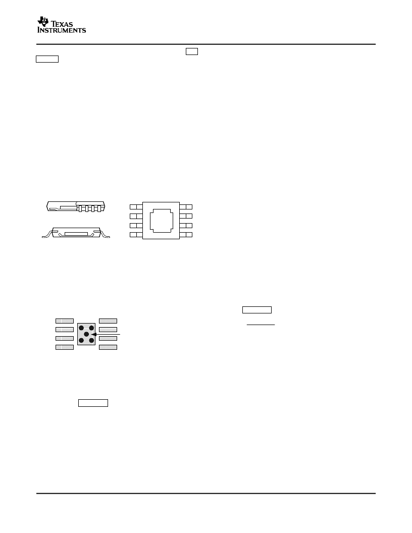
DIE
Side View (a)
DIE
End View (b)
Thermal
Pad
Bottom View (c)
Single or Dual
68 Mils x 70 Mils
(Via Diameter = 13 Mils)
P
D
T
max
T
A
JA
where
P
D
= Maximum power dissipation of THS4211 (watts)
T
MAX
= Absolute maximum junction temperature (150
°
C)
T
A
= Free-ambient temperature (
°
C)
θ
JA
=
θ
JC
+
θ
CA
θ
JC
= Thermal coefficient from junction to the case
θ
CA
= Thermal coefficient from the case to ambient air
(
°
C/W).
(6)
PowerPAD PCB LAYOUT CONSIDERATIONS
1. Prepare the PCB with a top side etch pattern as
shown in Figure 90. There should be etching for
the leads as well as etch for the thermal pad.
2. Place five holes in the area of the thermal pad.
These holes should be 13 mils in diameter. Keep
them small so that solder wicking through the
holes is not a problem during reflow.
3. Additional vias may be placed anywhere along
the thermal plane outside of the thermal pad
area. They help dissipate the heat generated by
the THS4211 and THS4215 IC. These additional
vias may be larger than the 13-mil diameter vias
THS4211
THS4215
SLOS400D–SEPTEMBER 2002–REVISED NOVEMBER 2004
pad on the underside of the package [see Fig-
ure 89(c)]. Because this thermal pad has direct
thermal contact with the die, excellent thermal per-
formance can be achieved by providing a good
thermal path away from the thermal pad.
directly under the thermal pad. They can be
larger because they are not in the thermal pad
area to be soldered, so wicking is not a problem.
4. Connect all holes to the internal ground plane.
5. When connecting these holes to the ground
plane,
do not
use the typical web or spoke via
connection methodology. Web connections have
a high thermal resistance connection that is
useful
for
slowing
the
soldering operations. This resistance makes the
soldering of vias that have plane connections
easier. In this application, however, low thermal
resistance is desired for the most efficient heat
transfer. Therefore, the holes under the THS4211
and THS4215 PowerPAD package should make
their connection to the internal ground plane, with
a complete connection around the entire circum-
ference of the plated-through hole.
6. The top-side solder mask should leave the ter-
minals of the package and the thermal pad area
with its five holes exposed. The bottom-side
solder mask should cover the five holes of the
thermal pad area. This prevents solder from
being pulled away from the thermal pad area
during the reflow process.
7. Apply solder paste to the exposed thermal pad
area and all of the IC terminals.
8. With these preparatory steps in place, the IC is
simply placed in position and run through the
solder reflow operation as any standard sur-
face-mount component. This results in a part that
is properly installed.
For a given
θ
, the maximum power dissipation is
shown in Figure 91 and is calculated by Equation 6:
The PowerPAD package allows both assembly and
thermal management in one manufacturing operation.
During the surface-mount solder operation (when the
leads are being soldered), the thermal pad can also
be soldered to a copper area underneath the pack-
age. Through the use of thermal paths within this
copper area, heat can be conducted away from the
package into either a ground plane or other heat
dissipating device.
heat
transfer
during
The PowerPAD package represents a breakthrough
in combining the small area and ease of assembly of
surface mount with the heretofore awkward mechan-
ical methods of heatsinking.
Figure 89. Views of Thermally
Enhanced Package
Although there are many ways to properly heatsink
the PowerPAD package, the following steps illustrate
the recommended approach.
Figure 90. PowerPAD PCB Etch and
Via Pattern
The next consideration is the package constraints.
The two sources of heat within an amplifier are
quiescent power and output power. The designer
should never forget about the quiescent heat gener-
ated within the device, especially multi-amplifier de-
vices. Because these devices have linear output
stages (Class AB), most of the heat dissipation is at
low output voltages with high output currents.
The other key factor when dealing with power dissi-
pation is how the devices are mounted on the PCB.
The PowerPAD devices are extremely useful for heat
dissipation.
But,
the
device
should
always
be
27
相關(guān)PDF資料 |
PDF描述 |
|---|---|
| THS5651ADW | 10-BIT, 125 MSPS, CommsDACE DIGITAL-TO-ANALOG CONVERTER |
| THS5651DW | 10-BIT, 100 MSPS, CommsDACE DIGITAL-TO-ANALOG CONVERTER |
| THS5651PW | 10-BIT, 100 MSPS, CommsDACE DIGITAL-TO-ANALOG CONVERTER |
| THS5661DW | 12-BIT, 100 MSPS, CommsDACE DIGITAL-TO-ANALOG CONVERTER |
| THS5661PW | 12-BIT, 100 MSPS, CommsDACE DIGITAL-TO-ANALOG CONVERTER |
相關(guān)代理商/技術(shù)參數(shù) |
參數(shù)描述 |
|---|---|
| THS4215DRBR | 功能描述:高速運算放大器 Super-Fast Ultr-Lo- Distortion Hi-Speed RoHS:否 制造商:Texas Instruments 通道數(shù)量:1 電壓增益 dB:116 dB 輸入補償電壓:0.5 mV 轉(zhuǎn)換速度:55 V/us 工作電源電壓:36 V 電源電流:7.5 mA 最大工作溫度:+ 85 C 安裝風格:SMD/SMT 封裝 / 箱體:SOIC-8 封裝:Tube |
| THS4215DRBRG4 | 功能描述:高速運算放大器 Super-Fast Ultr-Lo- Distortion Hi-Speed RoHS:否 制造商:Texas Instruments 通道數(shù)量:1 電壓增益 dB:116 dB 輸入補償電壓:0.5 mV 轉(zhuǎn)換速度:55 V/us 工作電源電壓:36 V 電源電流:7.5 mA 最大工作溫度:+ 85 C 安裝風格:SMD/SMT 封裝 / 箱體:SOIC-8 封裝:Tube |
| THS4215DRBT | 功能描述:高速運算放大器 Super-Fast Ultr-Lo- Distortion Hi-Speed RoHS:否 制造商:Texas Instruments 通道數(shù)量:1 電壓增益 dB:116 dB 輸入補償電壓:0.5 mV 轉(zhuǎn)換速度:55 V/us 工作電源電壓:36 V 電源電流:7.5 mA 最大工作溫度:+ 85 C 安裝風格:SMD/SMT 封裝 / 箱體:SOIC-8 封裝:Tube |
| THS4215DRBTG4 | 功能描述:高速運算放大器 Super-Fast Ultr-Lo- Distortion Hi-Speed RoHS:否 制造商:Texas Instruments 通道數(shù)量:1 電壓增益 dB:116 dB 輸入補償電壓:0.5 mV 轉(zhuǎn)換速度:55 V/us 工作電源電壓:36 V 電源電流:7.5 mA 最大工作溫度:+ 85 C 安裝風格:SMD/SMT 封裝 / 箱體:SOIC-8 封裝:Tube |
| THS4215DRG4 | 功能描述:高速運算放大器 Super-Fast Ultr-Lo- Distortion Hi-Speed RoHS:否 制造商:Texas Instruments 通道數(shù)量:1 電壓增益 dB:116 dB 輸入補償電壓:0.5 mV 轉(zhuǎn)換速度:55 V/us 工作電源電壓:36 V 電源電流:7.5 mA 最大工作溫度:+ 85 C 安裝風格:SMD/SMT 封裝 / 箱體:SOIC-8 封裝:Tube |
發(fā)布緊急采購,3分鐘左右您將得到回復(fù)。