- 您現(xiàn)在的位置:買賣IC網(wǎng) > PDF目錄383997 > THS4215DGNR (Texas Instruments, Inc.) LOW-DISTORTION HIGH-SPEED VOLTAGE FEEDBACK AMPLIFIER PDF資料下載
參數(shù)資料
| 型號: | THS4215DGNR |
| 廠商: | Texas Instruments, Inc. |
| 英文描述: | LOW-DISTORTION HIGH-SPEED VOLTAGE FEEDBACK AMPLIFIER |
| 中文描述: | 低失真高速電壓反饋型放大器 |
| 文件頁數(shù): | 25/41頁 |
| 文件大小: | 1591K |
| 代理商: | THS4215DGNR |
第1頁第2頁第3頁第4頁第5頁第6頁第7頁第8頁第9頁第10頁第11頁第12頁第13頁第14頁第15頁第16頁第17頁第18頁第19頁第20頁第21頁第22頁第23頁第24頁當前第25頁第26頁第27頁第28頁第29頁第30頁第31頁第32頁第33頁第34頁第35頁第36頁第37頁第38頁第39頁第40頁第41頁
www.ti.com
_
+
R
f
4kT = 1.6E-20J
at 290K
THS4211/THS4215
I
BN
E
O
E
RF
R
S
E
RS
I
BI
R
g
E
NI
4kTR
S
4kT
R
g
4kTR
f
E
O
E
2
NI
I
BN
R
S
2
4kTR
S
NG
2
I
BI
R
f
2
4kTR
f
NG
E
O
E
2
NI
I
BN
R
S
2
4kTR
S
I
BI
R
f
NG
2
4kTR
f
NG
Driving Capacitive Loads
-3
-2.5
-2
-1.5
-1
-0.5
0
0.5
1
100 k
1 M
10 M
100 M
1 G
Capacitive Load - Hz
N
FREQUENCY RESPONSE
vs
CAPACITIVE LOAD
R
(ISO)
= 15
L
= 50 pF
V
S
=
±
5 V
R
(ISO)
= 10
C
L
= 100 pF
R
(ISO)
= 25
C
L
= 10 pF
BOARD LAYOUT
Achieving optimum performance with a high fre-
quency amplifier like the THS4211 requires careful
attention to board layout parasitics and external
component types.
THS4211
THS4215
SLOS400D–SEPTEMBER 2002–REVISED NOVEMBER 2004
The Typical Characteristics show the recommended
isolation resistor vs capacitive load and the resulting
frequency response at the load. Parasitic capacitive
loads greater than 2 pF can begin to degrade the
performance of the THS4211. Long PC board traces,
unmatched cables, and connections to multiple de-
vices can easily cause this value to be exceeded.
Always consider this effect carefully, and add the
recommended series resistor as close as possible to
the
THS4211
output
pin
Guidelines).
(see
Board
Layout
The criterion for setting this R
resistor is a
maximum bandwidth, flat frequency response at the
load. For a gain of +2, the frequency response at the
output pin is already slightly peaked without the
capacitive load, requiring relatively high values of
R
(ISO)
to flatten the response at the load. Increasing
the noise gain also reduces the peaking.
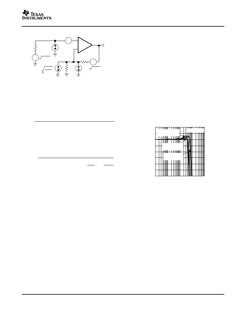
Figure 87. Noise Analysis Model
The total output shot noise voltage can be computed
as the square of all square output noise voltage
contributors. Equation 4 shows the general form for
the output noise voltage using the terms shown in
Equation 4:
(4)
Dividing this expression by the noise gain (NG=(1+
R
f
/R
g
)) gives the equivalent input-referred spot noise
voltage at the noninverting input, as shown in
Equation 5:
(5)
One of the most demanding, and yet very common,
load conditions for an op amp is capacitive loading.
Often, the capacitive load is the input of an A/D
converter, including additional external capacitance,
which may be recommended to improve A/D linearity.
A high-speed, high open-loop gain amplifier like the
THS4211 can be very susceptible to decreased
stability and closed-loop response peaking when a
capacitive load is placed directly on the output pin.
When the amplifier's open-loop output resistance is
considered, this capacitive load introduces an ad-
ditional pole in the signal path that can decrease the
phase margin. When the primary considerations are
frequency response flatness, pulse response fidelity,
or distortion, the simplest and most effective solution
is to isolate the capacitive load from the feedback
loop by inserting a series isolation resistor between
the amplifier output and the capacitive load. This
does not eliminate the pole from the loop response,
but rather shifts it and adds a zero at a higher
frequency. The additional zero acts to cancel the
phase lag from the capacitive load pole, thus increas-
ing the phase margin and improving stability.
Figure 88. Isolation Resistor Diagram
Recommendations that optimize performance include
the following:
1.
Minimize parasitic capacitance to any ac
ground for all of the signal I/O pins.
Parasitic
capacitance on the output and inverting input pins
can cause instability: on the noninverting input, it
can react with the source impedance to cause
unintentional band limiting. To reduce unwanted
capacitance, a window around the signal I/O pins
should be opened in all of the ground and power
planes around those pins. Otherwise, ground and
power planes should be unbroken elsewhere on
the board.
25
相關(guān)PDF資料 |
PDF描述 |
|---|---|
| THS4215DGNRG4 | LOW-DISTORTION HIGH-SPEED VOLTAGE FEEDBACK AMPLIFIER |
| THS4215DRB | LOW-DISTORTION HIGH-SPEED VOLTAGE FEEDBACK AMPLIFIER |
| THS5651ADW | 10-BIT, 125 MSPS, CommsDACE DIGITAL-TO-ANALOG CONVERTER |
| THS5651DW | 10-BIT, 100 MSPS, CommsDACE DIGITAL-TO-ANALOG CONVERTER |
| THS5651PW | 10-BIT, 100 MSPS, CommsDACE DIGITAL-TO-ANALOG CONVERTER |
相關(guān)代理商/技術(shù)參數(shù) |
參數(shù)描述 |
|---|---|
| THS4215DGNRG4 | 功能描述:高速運算放大器 Super-Fast Ultr-Lo- Distortion Hi-Speed RoHS:否 制造商:Texas Instruments 通道數(shù)量:1 電壓增益 dB:116 dB 輸入補償電壓:0.5 mV 轉(zhuǎn)換速度:55 V/us 工作電源電壓:36 V 電源電流:7.5 mA 最大工作溫度:+ 85 C 安裝風格:SMD/SMT 封裝 / 箱體:SOIC-8 封裝:Tube |
| THS4215DR | 功能描述:高速運算放大器 Super-Fast Ultr-Lo- Distortion Hi-Speed RoHS:否 制造商:Texas Instruments 通道數(shù)量:1 電壓增益 dB:116 dB 輸入補償電壓:0.5 mV 轉(zhuǎn)換速度:55 V/us 工作電源電壓:36 V 電源電流:7.5 mA 最大工作溫度:+ 85 C 安裝風格:SMD/SMT 封裝 / 箱體:SOIC-8 封裝:Tube |
| THS4215DRB | 制造商:Rochester Electronics LLC 功能描述:- Bulk |
| THS4215DRBR | 功能描述:高速運算放大器 Super-Fast Ultr-Lo- Distortion Hi-Speed RoHS:否 制造商:Texas Instruments 通道數(shù)量:1 電壓增益 dB:116 dB 輸入補償電壓:0.5 mV 轉(zhuǎn)換速度:55 V/us 工作電源電壓:36 V 電源電流:7.5 mA 最大工作溫度:+ 85 C 安裝風格:SMD/SMT 封裝 / 箱體:SOIC-8 封裝:Tube |
| THS4215DRBRG4 | 功能描述:高速運算放大器 Super-Fast Ultr-Lo- Distortion Hi-Speed RoHS:否 制造商:Texas Instruments 通道數(shù)量:1 電壓增益 dB:116 dB 輸入補償電壓:0.5 mV 轉(zhuǎn)換速度:55 V/us 工作電源電壓:36 V 電源電流:7.5 mA 最大工作溫度:+ 85 C 安裝風格:SMD/SMT 封裝 / 箱體:SOIC-8 封裝:Tube |
發(fā)布緊急采購,3分鐘左右您將得到回復。