- 您現(xiàn)在的位置:買賣IC網(wǎng) > PDF目錄98217 > THS1030CPWRG4 (TEXAS INSTRUMENTS INC) 1-CH 10-BIT PROPRIETARY METHOD ADC, PARALLEL ACCESS, PDSO28 PDF資料下載
參數(shù)資料
| 型號: | THS1030CPWRG4 |
| 廠商: | TEXAS INSTRUMENTS INC |
| 元件分類: | ADC |
| 英文描述: | 1-CH 10-BIT PROPRIETARY METHOD ADC, PARALLEL ACCESS, PDSO28 |
| 封裝: | GREEN, PLASTIC, TSSOP-28 |
| 文件頁數(shù): | 33/37頁 |
| 文件大?。?/td> | 727K |
| 代理商: | THS1030CPWRG4 |
第1頁第2頁第3頁第4頁第5頁第6頁第7頁第8頁第9頁第10頁第11頁第12頁第13頁第14頁第15頁第16頁第17頁第18頁第19頁第20頁第21頁第22頁第23頁第24頁第25頁第26頁第27頁第28頁第29頁第30頁第31頁第32頁當(dāng)前第33頁第34頁第35頁第36頁第37頁
THS1030
3V TO 5.5V, 10BIT, 30 MSPS
CMOS ANALOGTODIGITAL CONVERTER
SLAS243E NOVEMBER 1999 REVISED DECEMBER 2003
5
POST OFFICE BOX 655303
DALLAS, TEXAS 75265
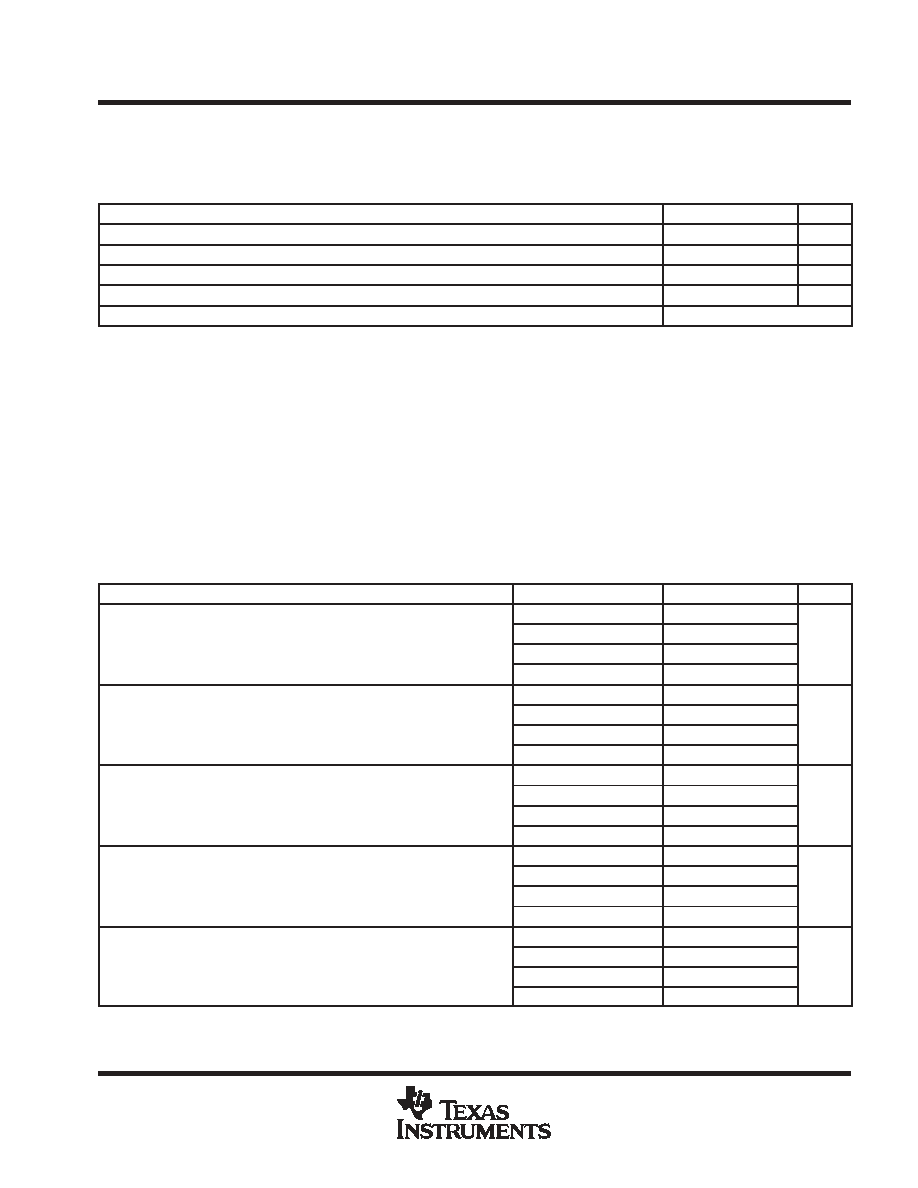
electrical characteristics over recommended operating conditions, AVDD = 3 V, DVDD = 3 V, fs = 30
MSPS/50% duty cycle, MODE = AVDD, 2-V input span from 0.5 V to 2.5 V, external reference,
TA = Tmin to Tmax (unless otherwise noted) (continued)
dc accuracy
PARAMETER
MIN
TYP
MAX
UNIT
INL
Integral nonlinearity (see Note 2)
±1
±2
LSB
DNL
Differential nonlinearity (see Note 3)
±0.3
±1
LSB
Offset error (see Note 4)
0.4
1.4
%FSR
Gain error (see Note 5)
1.4
3.5
%FSR
Missing code
No missing code assured
NOTES:
2. Integral nonlinearity refers to the deviation of each individual code from a line drawn from zero to full scale. The point used as zero
occurs 1/2 LSB before the first code transition. The full-scale point is defined as a level 1/2 LSB beyond the last code transition. The
deviation is measured from the center of each particular code to the true straight line between these two endpoints.
3. An ideal ADC exhibits code transitions that are exactly 1 LSB apart. DNL is the deviation from this ideal value. Therefore this measure
indicates how uniform the transfer function step sizes are. The ideal step size is defined here as the step size for the device under
test (i.e., (last transition level – first transition level)
÷ (2 n – 2)). Using this definition for DNL separates the effects of gain and offset
error. A minimum DNL better than –1 LSB ensures no missing codes.
4. Offset error is defined as the difference in analog input voltage – between the ideal voltage and the actual voltage – that will switch
the ADC output from code 0 to code 1. The ideal voltage level is determined by adding the voltage corresponding to 1/2 LSB to the
bottom reference level. The voltage corresponding to 1 LSB is found from the difference of top and bottom references divided by
the number of ADC output levels (1024).
5. Gain error is defined as the difference in analog input voltage – between the ideal voltage and the actual voltage – that will switch
the ADC output from code 1022 to code 1023. The ideal voltage level is determined by subtracting the voltage corresponding to 1.5
LSB from the top reference level. The voltage corresponding to 1 LSB is found from the difference of top and bottom references
divided by the number of ADC output levels (1024).
dynamic performance (See Note 6)
PARAMETER
TEST CONDITIONS
MIN
TYP
MAX
UNIT
f = 3.5 MHz
8.4
9
ENOB
Effective number of bits
f = 3.5 MHz, AVDD = 5 V
9
Bits
ENOB
Effective number of bits
f = 15 MHz, 3 V
7.8
Bits
f = 15 MHz, AVDD = 5 V
7.7
f = 3.5 MHz
56
60.6
SFDR
Spurious free dynamic range
f = 3.5 MHz, AVDD = 5 V
64.6
dB
SFDR
Spurious free dynamic range
f = 15 MHz
48.5
dB
f = 15 MHz, AVDD = 5 V
53
f = 3.5 MHz
60
56
dB
THD
Total harmonic distortion
f = 3.5 MHz, AVDD = 5 V
66.9
dB
THD
Total harmonic distortion
f = 15 MHz
47.5
f = 15 MHz, AVDD = 5 V
53.1
f = 3.5 MHz
53
57
dB
SNR
Signal-to-noise ratio
f = 3.5 MHz, AVDD = 5 V
56
dB
SNR
Signal-to-noise ratio
f = 15 MHz
53.1
f = 15 MHz, AVDD = 5 V
49.4
f = 3.5 MHz
52.5
56
SINAD
Signal-to-noise and distortion
f = 3.5 MHz, AVDD = 5 V
56
dB
SINAD
Signal-to-noise and distortion
f = 15 MHz
48.6
dB
f = 15 MHz, AVDD = 5 V
48.1
NOTES:
6. Input amplitude of single tone sine wave for dynamic tests is 0.5 dBFS.
相關(guān)PDF資料 |
PDF描述 |
|---|---|
| THS1030IPWR | 1-CH 10-BIT PROPRIETARY METHOD ADC, PARALLEL ACCESS, PDSO28 |
| THS1030CDWG4 | 1-CH 10-BIT PROPRIETARY METHOD ADC, PARALLEL ACCESS, PDSO28 |
| THS1030IDW | 1-CH 10-BIT PROPRIETARY METHOD ADC, PARALLEL ACCESS, PDSO28 |
| THS1030CPWR | 1-CH 10-BIT PROPRIETARY METHOD ADC, PARALLEL ACCESS, PDSO28 |
| THS1030IDWRG4 | 1-CH 10-BIT PROPRIETARY METHOD ADC, PARALLEL ACCESS, PDSO28 |
相關(guān)代理商/技術(shù)參數(shù) |
參數(shù)描述 |
|---|---|
| THS1030EVM | 功能描述:數(shù)據(jù)轉(zhuǎn)換 IC 開發(fā)工具 THS1030 Eval Mod RoHS:否 制造商:Texas Instruments 產(chǎn)品:Demonstration Kits 類型:ADC 工具用于評估:ADS130E08 接口類型:SPI 工作電源電壓:- 6 V to + 6 V |
| THS1030IDW | 功能描述:模數(shù)轉(zhuǎn)換器 - ADC _ RoHS:否 制造商:Texas Instruments 通道數(shù)量:2 結(jié)構(gòu):Sigma-Delta 轉(zhuǎn)換速率:125 SPs to 8 KSPs 分辨率:24 bit 輸入類型:Differential 信噪比:107 dB 接口類型:SPI 工作電源電壓:1.7 V to 3.6 V, 2.7 V to 5.25 V 最大工作溫度:+ 85 C 安裝風(fēng)格:SMD/SMT 封裝 / 箱體:VQFN-32 |
| THS1030IDWG4 | 功能描述:模數(shù)轉(zhuǎn)換器 - ADC 10-Bit 30 MSPS 1-Ch Pin Comp RoHS:否 制造商:Texas Instruments 通道數(shù)量:2 結(jié)構(gòu):Sigma-Delta 轉(zhuǎn)換速率:125 SPs to 8 KSPs 分辨率:24 bit 輸入類型:Differential 信噪比:107 dB 接口類型:SPI 工作電源電壓:1.7 V to 3.6 V, 2.7 V to 5.25 V 最大工作溫度:+ 85 C 安裝風(fēng)格:SMD/SMT 封裝 / 箱體:VQFN-32 |
| THS1030IDWR | 功能描述:視頻模擬/數(shù)字化轉(zhuǎn)換器集成電路 10-Bit 30 MSPS 1-Ch Pin Comp RoHS:否 制造商:Texas Instruments 輸入信號類型:Differential 轉(zhuǎn)換器數(shù)量:1 ADC 輸入端數(shù)量:4 轉(zhuǎn)換速率:3 Gbps 分辨率:8 bit 結(jié)構(gòu): 輸入電壓:3.3 V 接口類型:SPI 信噪比: 電壓參考: 電源電壓-最大:3.45 V 電源電壓-最小:3.15 V 最大功率耗散: 最大工作溫度:+ 85 C 最小工作溫度:- 40 C 封裝 / 箱體:TCSP-48 封裝:Reel |
| THS1030IDWRG4 | 功能描述:視頻模擬/數(shù)字化轉(zhuǎn)換器集成電路 10-Bit 30 MSPS 1-Ch Pin Comp RoHS:否 制造商:Texas Instruments 輸入信號類型:Differential 轉(zhuǎn)換器數(shù)量:1 ADC 輸入端數(shù)量:4 轉(zhuǎn)換速率:3 Gbps 分辨率:8 bit 結(jié)構(gòu): 輸入電壓:3.3 V 接口類型:SPI 信噪比: 電壓參考: 電源電壓-最大:3.45 V 電源電壓-最小:3.15 V 最大功率耗散: 最大工作溫度:+ 85 C 最小工作溫度:- 40 C 封裝 / 箱體:TCSP-48 封裝:Reel |
發(fā)布緊急采購,3分鐘左右您將得到回復(fù)。