- 您現(xiàn)在的位置:買賣IC網(wǎng) > PDF目錄98217 > THS1030CDW (TEXAS INSTRUMENTS INC) 1-CH 10-BIT PROPRIETARY METHOD ADC, PARALLEL ACCESS, PDSO28 PDF資料下載
參數(shù)資料
| 型號: | THS1030CDW |
| 廠商: | TEXAS INSTRUMENTS INC |
| 元件分類: | ADC |
| 英文描述: | 1-CH 10-BIT PROPRIETARY METHOD ADC, PARALLEL ACCESS, PDSO28 |
| 封裝: | GREEN, PLASTIC, SOIC-28 |
| 文件頁數(shù): | 21/37頁 |
| 文件大小: | 727K |
| 代理商: | THS1030CDW |
第1頁第2頁第3頁第4頁第5頁第6頁第7頁第8頁第9頁第10頁第11頁第12頁第13頁第14頁第15頁第16頁第17頁第18頁第19頁第20頁當(dāng)前第21頁第22頁第23頁第24頁第25頁第26頁第27頁第28頁第29頁第30頁第31頁第32頁第33頁第34頁第35頁第36頁第37頁
THS1030
3V TO 5.5V, 10BIT, 30 MSPS
CMOS ANALOGTODIGITAL CONVERTER
SLAS243E NOVEMBER 1999 REVISED DECEMBER 2003
28
POST OFFICE BOX 655303
DALLAS, TEXAS 75265
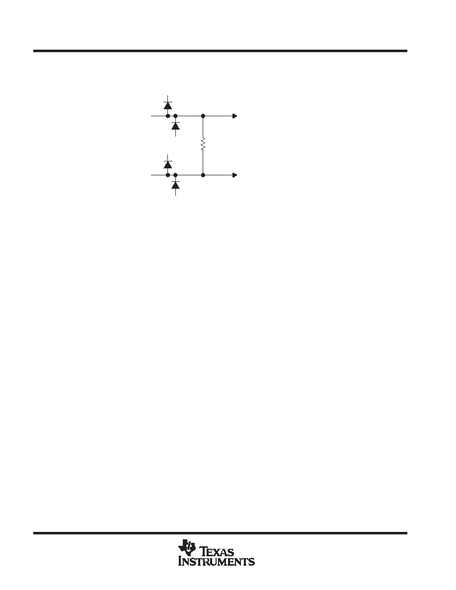
driving REFTF and REFBF (full external reference mode)
AVDD
AGND
AVDD
AGND
680 R
To REFBS
(For Kelvin Connection)
To REFTS
(For Kelvin Connection)
REFTF
REFBF
Figure 33. Equivalent Circuit of REFTF and REFBF Inputs
Note the need for off-chip decoupling.
driving the clock input
Obtaining good performance from the THS1030 requires care when driving the clock input.
Different sections of the sample-and-hold and ADC operate while the clock is low or high. The user should
ensure that the clock duty cycle remains near 50% to ensure that all internal circuits have as much time as
possible in which to operate.
The CLK pin should be driven from a low jitter source for best dynamic performance. To maintain low jitter at
the CLK input, any clock buffers external to the THS1030 should have fast rising edges. Use a fast logic family
such as AC or ACT to drive the CLK pin, and consider powering any clock buffers separately from any other
logic on the PCB to prevent digital supply noise appearing on the buffered clock edges as jitter.
The CLK input threshold is nominally around AVDD/2—ensure that any clock buffers have an appropriate supply
voltage to drive above and below this level.
digital output loading and circuit board layout
The THS1030 outputs are capable of driving rail-to-rail with up to 20 pF of load per pin at 30-MHz clock and 3-V
digital supply. Minimizing the load on the outputs will improve THS1030 signal-to-noise performance by
reducing the switching noise coupling from the THS1030 output buffers to the internal analog circuits. The
output load capacitance can be minimized by buffering the THS1030 digital outputs with a low input capacitance
buffer placed as close to the output pins as physically possible, and by using the shortest possible tracks
between the THS1030 and this buffer.
Noise levels at the output buffers, and hence coupling to the analog circuits within THS1030, becomes worse
as the THS1030 digital supply voltage is increased. Where possible, consider using the lowest DVDD that the
application can tolerate.
Use good layout practices when designing the application PCB to ensure that any off-chip return currents from
the THS1030 digital outputs (and any other digital circuits on the PCB) do not return via the supplies to any
sensitive analog circuits. The THS1030 should be soldered directly to the PCB for best performance. Socketing
the device will degrade performance by adding parasitic socket inductance and capacitance to all pins.
相關(guān)PDF資料 |
PDF描述 |
|---|---|
| THS1030IDWR | 1-CH 10-BIT PROPRIETARY METHOD ADC, PARALLEL ACCESS, PDSO28 |
| THS1030CPW | 1-CH 10-BIT PROPRIETARY METHOD ADC, PARALLEL ACCESS, PDSO28 |
| THS1030IPW | 1-CH 10-BIT PROPRIETARY METHOD ADC, PARALLEL ACCESS, PDSO28 |
| THS1030IDWG4 | 1-CH 10-BIT PROPRIETARY METHOD ADC, PARALLEL ACCESS, PDSO28 |
| THS1030CDWR | 1-CH 10-BIT PROPRIETARY METHOD ADC, PARALLEL ACCESS, PDSO28 |
相關(guān)代理商/技術(shù)參數(shù) |
參數(shù)描述 |
|---|---|
| THS1030CDWG4 | 功能描述:模數(shù)轉(zhuǎn)換器 - ADC 10-Bit 30 MSPS 1-Ch Pin Comp RoHS:否 制造商:Texas Instruments 通道數(shù)量:2 結(jié)構(gòu):Sigma-Delta 轉(zhuǎn)換速率:125 SPs to 8 KSPs 分辨率:24 bit 輸入類型:Differential 信噪比:107 dB 接口類型:SPI 工作電源電壓:1.7 V to 3.6 V, 2.7 V to 5.25 V 最大工作溫度:+ 85 C 安裝風(fēng)格:SMD/SMT 封裝 / 箱體:VQFN-32 |
| THS1030CDWR | 功能描述:模數(shù)轉(zhuǎn)換器 - ADC 10-Bit 30 MSPS 1-Ch Pin Comp RoHS:否 制造商:Texas Instruments 通道數(shù)量:2 結(jié)構(gòu):Sigma-Delta 轉(zhuǎn)換速率:125 SPs to 8 KSPs 分辨率:24 bit 輸入類型:Differential 信噪比:107 dB 接口類型:SPI 工作電源電壓:1.7 V to 3.6 V, 2.7 V to 5.25 V 最大工作溫度:+ 85 C 安裝風(fēng)格:SMD/SMT 封裝 / 箱體:VQFN-32 |
| THS1030CDWRG4 | 功能描述:模數(shù)轉(zhuǎn)換器 - ADC 10-Bit 30 MSPS 1-Ch Pin Comp RoHS:否 制造商:Texas Instruments 通道數(shù)量:2 結(jié)構(gòu):Sigma-Delta 轉(zhuǎn)換速率:125 SPs to 8 KSPs 分辨率:24 bit 輸入類型:Differential 信噪比:107 dB 接口類型:SPI 工作電源電壓:1.7 V to 3.6 V, 2.7 V to 5.25 V 最大工作溫度:+ 85 C 安裝風(fēng)格:SMD/SMT 封裝 / 箱體:VQFN-32 |
| THS1030CPW | 功能描述:模數(shù)轉(zhuǎn)換器 - ADC 10-Bit 30 MSPS 1-Ch Pin Comp RoHS:否 制造商:Texas Instruments 通道數(shù)量:2 結(jié)構(gòu):Sigma-Delta 轉(zhuǎn)換速率:125 SPs to 8 KSPs 分辨率:24 bit 輸入類型:Differential 信噪比:107 dB 接口類型:SPI 工作電源電壓:1.7 V to 3.6 V, 2.7 V to 5.25 V 最大工作溫度:+ 85 C 安裝風(fēng)格:SMD/SMT 封裝 / 箱體:VQFN-32 |
| THS1030CPWG4 | 功能描述:模數(shù)轉(zhuǎn)換器 - ADC 10-Bit 30 MSPS 1-Ch Pin Comp RoHS:否 制造商:Texas Instruments 通道數(shù)量:2 結(jié)構(gòu):Sigma-Delta 轉(zhuǎn)換速率:125 SPs to 8 KSPs 分辨率:24 bit 輸入類型:Differential 信噪比:107 dB 接口類型:SPI 工作電源電壓:1.7 V to 3.6 V, 2.7 V to 5.25 V 最大工作溫度:+ 85 C 安裝風(fēng)格:SMD/SMT 封裝 / 箱體:VQFN-32 |
發(fā)布緊急采購,3分鐘左右您將得到回復(fù)。