- 您現(xiàn)在的位置:買賣IC網(wǎng) > PDF目錄385924 > TH6503 (Electronic Theatre Controls, Inc.) USB Low-Speed Interface PDF資料下載
參數(shù)資料
| 型號(hào): | TH6503 |
| 廠商: | Electronic Theatre Controls, Inc. |
| 英文描述: | USB Low-Speed Interface |
| 中文描述: | USB低速接口 |
| 文件頁(yè)數(shù): | 11/24頁(yè) |
| 文件大小: | 342K |
| 代理商: | TH6503 |
第1頁(yè)第2頁(yè)第3頁(yè)第4頁(yè)第5頁(yè)第6頁(yè)第7頁(yè)第8頁(yè)第9頁(yè)第10頁(yè)當(dāng)前第11頁(yè)第12頁(yè)第13頁(yè)第14頁(yè)第15頁(yè)第16頁(yè)第17頁(yè)第18頁(yè)第19頁(yè)第20頁(yè)第21頁(yè)第22頁(yè)第23頁(yè)第24頁(yè)
11
TH6503 USB Low-Speed Interface
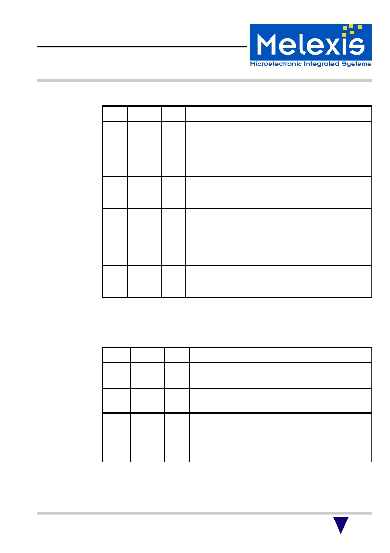
CntOutRegister
(read only)
second byte of each out transfer following an OUT packet sync
Adr/CntInRegister
(write only)
first byte of each data in transfer following the IN packet sync
Register
Description
(continued)
Internal Register
Bit
Number
Bit
Mnemonic
Reset
Status
Function
7-6
OA
0
OUT Address
last valid OUT endpoint
indicates the endpoint of actual OUT FIFO data
00 EP0
01 EP1
10 EP2
only valid if EP1 OUT or EP2 OUT enabled, otherwise the internal
Revision number is visible
5
TO
0
Toggle OUT
is set if the data packet PID was DATA1 and reset if the data packet
PID was DATA0
is latched with a valid EP0 SETUP or a OUT Token
4
SET
0
Setup
is set if a SETUP token is received
is reset after OUT transfer to microcontroller
no STALL or NAK is sent because it is not permitted on the SETUP
token
the SO0 and SI0 (STALL EP0) flags in the USBFlagRegister are reset
on rising edge of Setup
a SETUP token flash all IN FIFOs
3-0
OC3-0
0
EP0 OUT Byte Count
amount of OUT data received in the EP0 FIFO in bytes
applicable values from 0 to 8
a zero data transfer is identified 0
Bit
Number
Bit
Mnemonic
Reset
Status
Function
7
TI
0
Toggle IN
is set if the data packet PID is DATA1 and reset if the data packet PID
is DATA0
6-4
RA2-0
0
Internal Address
destination address for a write operation to a TH6503 register or IN
FIIFO
3-0
IC3-0
0
IN Byte Count
number of data bytes to be transmitted without Adr/CntInRegister from
the microcontroller to the TH6503 if the destination address was an IN
FIFO
applicable values from 0 to 8
0 indicates a zero data transfer to the USB host, but blocks the InFIFO
until ACK is received
相關(guān)PDF資料 |
PDF描述 |
|---|---|
| TH71112 | 868/915MHz FSK/FM/ASK Receiver |
| TH7120 | 300 to 930MHz FSK/FM/ASK Transceiver |
| TH9030 | 14 pin DIP, 5.0 Volt, HCMOS/TTL, Clock Oscillator |
| THAT2150A | IC Voltage-Controlled Amplifiers |
| THAT2151 | IC Voltage-Controlled Amplifiers |
相關(guān)代理商/技術(shù)參數(shù) |
參數(shù)描述 |
|---|---|
| TH65-930 | 制造商:C&K Components 功能描述: |
| TH-66006 | 制造商:GC Electronics 功能描述: |
| TH-66009 | 制造商:GC Electronics 功能描述: |
| TH6A | 制造商:TOPSTEK 制造商全稱:TOPSTEK 功能描述:Topstek Current Transducer |
| TH6A-B12 | 制造商:TOPSTEK 制造商全稱:TOPSTEK 功能描述:Topstek Current Transducer |
發(fā)布緊急采購(gòu),3分鐘左右您將得到回復(fù)。