- 您現(xiàn)在的位置:買賣IC網(wǎng) > PDF目錄98215 > TFP201CPZP (TEXAS INSTRUMENTS INC) SPECIALTY CONSUMER CIRCUIT, PQFP100 PDF資料下載
參數(shù)資料
| 型號: | TFP201CPZP |
| 廠商: | TEXAS INSTRUMENTS INC |
| 元件分類: | 消費(fèi)家電 |
| 英文描述: | SPECIALTY CONSUMER CIRCUIT, PQFP100 |
| 封裝: | 14 X 14 MM, 1.40 MM HEIGHT, 0.50 MM PITCH, POWER, THERMALLY ENHANCED, PLASTIC, TQFP-100 |
| 文件頁數(shù): | 17/22頁 |
| 文件大小: | 286K |
| 代理商: | TFP201CPZP |
TFP201, TFP201A
TI PanelBus
DIGITAL RECEIVER
SLDS116 - MARCH 2000
4
POST OFFICE BOX 655303
DALLAS, TEXAS 75265
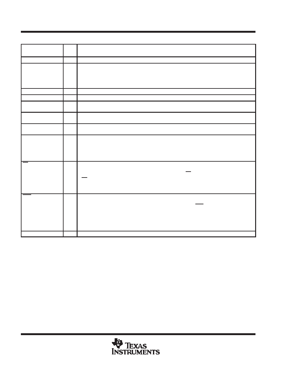
Terminal Functions (continued)
TERMINAL
I/O
DESCRIPTION
NAME
NO.
I/O
DESCRIPTION
DVDD
6,38,67
VDD
Digital VDD – Power supply for digital core. Nominally 3.3 V
EXT_RES
96
AI
Impedance matching control – An external resistor tied to this pin and AVDD will set the receiver input
termination resistance. The external resistor’s value should be 10x the cable’s single-ended characteristic
impedance, Zo. (Example: If a 500-
twisted pair cable is used, its single-ended characteristic impedance,
Zo, is 50
. A 500- resistor should be connected to EXT_RES and AVDD to set the single-ended receiver
input resistance to 50-
.)
HSYNC
48
DO
Horizontal sync output
RSVD
99
DI
Reserved. Must be tied high for normal operation.
OVDD
18,29,43,
57,78
VDD
Output driver VDD – Power supply for output drivers. Nominally 3.3 V
ODCK
44
DO
Output data clock - Pixel clock. All pixel outputs QE[23:0] and QO[23:0] (if in 2-pixel/clock mode) along with
DE, HSYNC, VSYNC and CTL[3:1] are synchronized to this clock.
OGND
19,28,45,
58,76
GND
Output driver ground – Ground reference and current return for digital output drivers
OCK_INV
100
DI
ODCK Polarity – Selects ODCK edge on which pixel data (QE[23:0] and QO[23:0]) and control signals
(HSYNC, VSYNC, DE, CTL1-3 ) are latched
Normal Mode:
High : Latches output data on rising ODCK edge
Low : Latches output data on falling ODCK edge
PD
2
DI
Power down – An active low signal that controls the TFP201/201A power-down state. During power down all
output buffers are switched to a high impedance state and brought low through a weak pulldown. All analog
circuits are powered down and all inputs are disabled, except for PD.
If PD is left unconnected an internal pullup will default the TFP201/201A to normal operation.
High : Normal operation
Low: Power down
PDO
9
DI
Output drive power down – An active low signal that controls the power-down state of the output drivers.
During output drive power down, the output drivers (except SCDT and CTL1) are driven to a high impedance
state. A weak pulldown will slowly pull these outputs to a low level. When PDO is left unconnected, an internal
pullup defaults the TFP201/201A to normal operation.
High : Normal operation/output drivers on
Low: Output drive power down.
PGND
98
GND
PLL GND – Ground reference and current return for internal PLL
ADV
ANCE
INFORMA
TION
相關(guān)PDF資料 |
PDF描述 |
|---|---|
| TFP401ACPZP | SPECIALTY CONSUMER CIRCUIT, PQFP100 |
| TFP401CPZP | SPECIALTY CONSUMER CIRCUIT, PQFP100 |
| TFP401AMPZPEP | SPECIALTY CONSUMER CIRCUIT, PQFP100 |
| TFP401APZP | SPECIALTY CONSUMER CIRCUIT, PQFP100 |
| TFP401APZPG4 | SPECIALTY CONSUMER CIRCUIT, PQFP100 |
相關(guān)代理商/技術(shù)參數(shù) |
參數(shù)描述 |
|---|---|
| TFP201PZP | 功能描述:顯示接口集成電路 PanelBus DVI Receiver 112MHz RoHS:否 制造商:Texas Instruments 電源電流:125 mA 工作溫度范圍:- 40 C to + 105 C 封裝 / 箱體:WQFN-60 封裝:Reel |
| TFP201PZPG4 | 功能描述:顯示接口集成電路 PanelBus DVI Rcvr RoHS:否 制造商:Texas Instruments 電源電流:125 mA 工作溫度范圍:- 40 C to + 105 C 封裝 / 箱體:WQFN-60 封裝:Reel |
| TFP2N60 | 制造商:TAK_CHEONG 制造商全稱:Tak Cheong Electronics (Holdings) Co.,Ltd 功能描述:N-Channel Power MOSFET 2.0A, 600V, 4.6Ω |
| TFP2N60A | 制造商:TAK_CHEONG 制造商全稱:Tak Cheong Electronics (Holdings) Co.,Ltd 功能描述:N-Channel Power MOSFET 2.1A, 600V, 5.6Ω |
| TFP2N65 | 制造商:TAK_CHEONG 制造商全稱:Tak Cheong Electronics (Holdings) Co.,Ltd 功能描述:N-Channel Power MOSFET 1.9A, 650V, 7.5?? |
發(fā)布緊急采購,3分鐘左右您將得到回復(fù)。