- 您現(xiàn)在的位置:買賣IC網(wǎng) > PDF目錄98190 > TDA4470-MFSY (ATMEL CORP) AM/FM, AUDIO/VIDEO DEMODULATOR, PDSO28 PDF資料下載
參數(shù)資料
| 型號: | TDA4470-MFSY |
| 廠商: | ATMEL CORP |
| 元件分類: | 接收器 |
| 英文描述: | AM/FM, AUDIO/VIDEO DEMODULATOR, PDSO28 |
| 封裝: | ROHS COMPLIANT, SSOP-28 |
| 文件頁數(shù): | 5/24頁 |
| 文件大?。?/td> | 350K |
| 代理商: | TDA4470-MFSY |

13
4803C–TVVCR–10/05
TDA4470
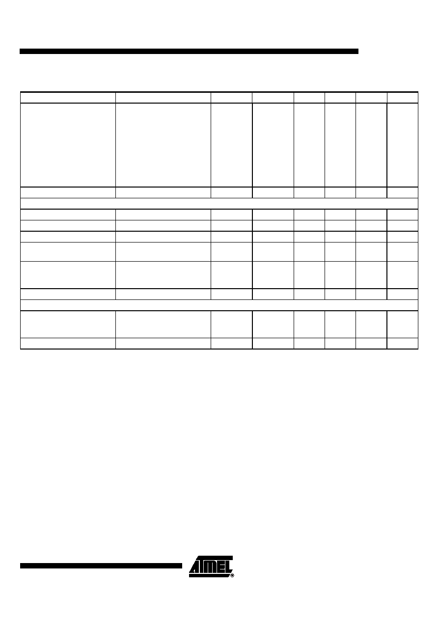
Weighted signal-to-noise ratio:
(CCIR 468)
Reference signal:
VIN = 10 mV
FM deviation = ±27 kHz
fmod = 1 kHz
tested with the double
FM demodulated U2860B
B/G modulated VIF signal
Black screen: Channel 1/2
Grid pattern: Channel 1/2
Grey screen 50%: Channel 1/2
S/N
60/58
54/52
60/57
dB
Ripple rejection
(1)
23, 24
RR
35
dB
AF Output-AM
25(11)
DC output voltage
VDC
2.2
V
Output resistance
(1)
ROUT
150
AF output voltage
VOAF
400
500
630
mVRMS
Total harmonic distortion
m = 54%
f
mod = 1 kHz and 12.5 kHz
THD
1
2
%
Signal to noise ratio
Reference: m = 54%,
f
mod = 1 kHz,
22 kHz low-pass filter
S/N
65
dB
Ripple rejection
Pin 23/pin 25(1)
RR
28
dB
SIF Input Selector Switch
3
Control voltage:
- input 1 active
- input 2 active
(12)
VSW
2.0
0
V
S
0.8
V
Switching current
ISW
±100
A
7.
Electrical Characteristics (Continued)
VS = +5V, Tamb = +25°C; reference point pin 4 (9, 16), unless otherwise specified.
Parameters
Test Conditions
Pin
Symbol
Min.
Typ.
Max.
Unit
Notes:
1. This parameter is given as an application information and has not been tested during production.
2. In VCR mode, the VIF- and SIF path is switched off.
3. The adjustment of the turn over point (delayed tuner AGC) with the external resistor R
TOP or external voltage VTOP is
possible.
4. Resonance circuit of VCO (fo = 38.9 MHz): CVCO = 8.2 - 10 pF,
Coil LVCO with unloaded Q-factor Q
o ≥ 60 for an oscillator voltage ≥ 100 mVRMS at pin 20 - 21
(e.g., TOKO coil 7 KM, 292 XNS - 4051Z).
5. The oscillator drift is related to the picture carrier frequency, given that the external LC circuit is temperature-compensated.
6.
α (1.07) = 20 log (4.43 MHz component/1.07 MHz component); α (1.07) value related to black-white signal
input signal conditions: picture carrier = 0 dB, colour carrier = –6 dB, sound carrier = –24 dB.
7. Without external control at pin 13 the IC automatically operates in mode 1:
negatively modulated video-IF signals and FM/NICAM sound signals.
8. Without a control voltage at pin 19 the falling AFC curve is automatically selected.
9. With an open circuit at pin 14 the L’ switch is not active.
10. Picture carrier PC = 38.9 MHz; sound carrier SC
1 = 33.4 MHz, SC2 = 33.16 MHz;
PC/SC1 =13 dB; PC/SC2 = 20 dB; PC unmodulated (equivalent to synchronous peak level).
11. Sound carrier SC = 32.4 MHz, modulated with f
mod = 1 kHz, m = 54%; VIN =10 mV
12. Without a control voltage at pin 3 the SIF input 1 is automatically selected.
相關(guān)PDF資料 |
PDF描述 |
|---|---|
| TDA4470-MSD | SPECIALTY CONSUMER CIRCUIT, PDIP28 |
| TDA4470-MFLG3 | SPECIALTY CONSUMER CIRCUIT, PDSO28 |
| TDA4470-MFSG3 | SPECIALTY CONSUMER CIRCUIT, PDSO28 |
| TDA4470-MFS | SPECIALTY CONSUMER CIRCUIT, PDSO28 |
| TDA4470-MSD | SPECIALTY CONSUMER CIRCUIT, PDIP28 |
相關(guān)代理商/技術(shù)參數(shù) |
參數(shù)描述 |
|---|---|
| TDA4470-MSD | 制造商:TEMIC 制造商全稱:TEMIC Semiconductors 功能描述:Multistandard Video-IF and Quasi Parallel Sound Processing |
| TDA4471 | 制造商:TEMIC 制造商全稱:TEMIC Semiconductors 功能描述:Multistandard Video-IF and Quasi Parallel Sound Processing |
| TDA4472 | 制造商:TEMIC 制造商全稱:TEMIC Semiconductors 功能描述:Video-IF and Quasi Parallel Sound Processing |
| TDA4472-A | 制造商:TEMIC 制造商全稱:TEMIC Semiconductors 功能描述:Video-IF (VIF) with FPLL Demodulation and Quasi Parallel Sound (QPS) Processing |
| TDA4472-M | 制造商:TEMIC 制造商全稱:TEMIC Semiconductors 功能描述:Video-IF and Quasi Parallel Sound Processing |
發(fā)布緊急采購,3分鐘左右您將得到回復(fù)。