- 您現(xiàn)在的位置:買賣IC網(wǎng) > PDF目錄383937 > TCM810RELB713 (Microchip Technology Inc.) 3-Pin Microcontroller Reset Monitors PDF資料下載
參數(shù)資料
| 型號: | TCM810RELB713 |
| 廠商: | Microchip Technology Inc. |
| 英文描述: | 3-Pin Microcontroller Reset Monitors |
| 中文描述: | 3引腳單片機復(fù)位監(jiān)控器 |
| 文件頁數(shù): | 2/16頁 |
| 文件大?。?/td> | 148K |
| 代理商: | TCM810RELB713 |
TCM809/TCM810
DS21661D-page 2
2005 Microchip Technology Inc.
1.0
ELECTRICAL
CHARACTERISTICS
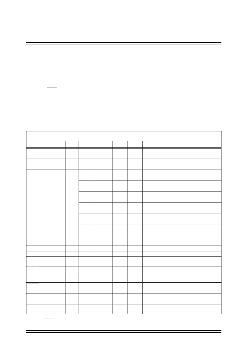
Absolute Maximum Ratings
Supply Voltage (V
DD
to GND) ........................................................6.0V
RESET, RESET ...................................................-0.3V to (V
DD
+0.3V)
Input Current, V
DD
.......................................................................20 mA
Output Current, RESET, RESET.................................................20 mA
dV/dt (V
DD
)...........................................................................100V/μsec
Operating Temperature Range ...................................-40°C to +125°C
Power Dissipation (T
= 70°C):
3-Pin SOT-23B (derate 4 mW/°C above +70°C)....................320 mW
3-Pin SC-70 (derate 2.17 mW/°C above +70°C)....................174 mW
Storage Temperature Range.......................................-65°C to +150°C
Maximum Junction Temperature, T
J
............................................150°C
Notice:
Stresses above those listed under “Maximum
Ratings” may cause permanent damage to the device. This is
a stress rating only and functional operation of the device at
those or any other conditions above those indicated in the
operational listings of this specification is not implied.
Exposure to maximum rating conditions for extended periods
may affect device reliability.
ELECTRICAL CHARACTERISTICS
V
DD
= Full Range, T
A
= Operating Temperature Range, unless otherwise noted. Typical values are at T
A
= +25°C,
V
DD
= 5V for L/M/J, 3.3V for T/S, 3.0V for R and 2.5V for Z
(Note 1)
.
Parameter
Sym
Min
Typ
Max
Units
Test Conditions
V
DD
Range
1.0
1.2
—
—
4.56
4.50
4.31
4.25
3.93
3.89
3.04
3.00
2.89
2.85
2.59
2.55
2.28
2.25
—
—
140
—
—
12
9
4.63
—
4.38
—
4.00
—
3.08
—
2.93
—
2.63
—
2.32
—
30
65
320
5.5
5.5
30
25
4.70
4.75
4.45
4.50
4.06
4.10
3.11
3.15
2.96
3.00
2.66
2.70
2.35
2.38
—
—
560
V
T
A
= 0°C to +70°C
T
A
= – 40°C to +125°C
TCM8xx
L/M/J:
TCM8xx
R/S/T/Z:
TCM8xx
L:
Supply Current
I
CC
μA
V
DD
< 5.5V
V
DD
< 3.6V
T
A
= +25°C
T
A
= – 40°C to +125°C
T
A
= +25°C
T
A
= – 40°C to +125°C
T
A
= +25°C
T
A
= – 40°C to +125°C
T
A
= +25°C
T
A
= – 40°C to +125°C
T
A
= +25°C
T
A
= – 40°C to +125°C
T
A
= +25°C
T
A
= – 40°C to +125°C
T
A
= +25°C
T
A
= – 40°C to +125°C
Reset Threshold
(Note 2)
V
TH
V
V
V
V
V
V
V
V
V
V
V
V
V
TCM8xx
M:
TCM809
J:
TCM8xx
T:
TCM8xx
S:
TCM8xx
R:
TCM8xx
Z:
Reset Threshold Tempco
V
DD
to Reset Delay,
Reset Active Time Out
Period
RESET Output Voltage
Low (
TCM809
)
ppm/°C
μsec
msec
V
DD
= V
TH
to (V
TH
– 100 mV)
(Note 2)
V
OL
—
—
—
—
—
—
—
—
—
—
—
0.3
0.4
0.3
—
—
0.3
0.4
—
V
TCM809
R/S/T/Z:
TCM809
L/M/J:
V
DD
> 1.0V, I
SINK
= 50 μA
TCM809
R/S/T/Z: V
DD
> V
TH
max, I
SOURCE
= 500 μA
TCM809
L/M/J: V
DD
> V
TH
max, I
SOURCE
= 800 μA
TCM810
R/S/T/Z:V
DD
= V
TH
max, I
SINK
= 1.2 mA
TCM810
L/M:
V
DD
= V
TH
max, I
SINK
= 3.2 mA
1.8 < V
DD
< V
TH
min, I
SOURCE
= 150 μA
V
DD
= V
TH
min, I
SINK
= 1.2 mA
V
DD
= V
TH
min, I
SINK
= 3.2 mA
RESET Output Voltage
High (
TCM809
)
V
OH
0.8 V
DD
V
DD
– 1.5
—
—
0.8 V
DD
V
RESET Output Voltage
Low (
TCM810
)
V
OL
V
RESET Output Voltage
High (
TCM810
)
Note
1:
Production testing done at T
= +25°C, overtemperature limits ensured by QC screen.
2:
RESET output for
TCM809
, RESET output for
TCM810
.
V
OH
V
相關(guān)PDF資料 |
PDF描述 |
|---|---|
| TCM810REN | 3-Pin Microcontroller Reset Monitors |
| TCM810RVB713 | 3-Pin Microcontroller Reset Monitors |
| TCM810RVLB713 | 3-Pin Microcontroller Reset Monitors |
| TCM810RVN | 3-Pin Microcontroller Reset Monitors |
| TCM809JEB713 | 3-Pin Microcontroller Reset Monitors |
相關(guān)代理商/技術(shù)參數(shù) |
參數(shù)描述 |
|---|---|
| TCM810REN | 制造商:MICROCHIP 制造商全稱:Microchip Technology 功能描述:3-Pin Microcontroller Reset Monitors |
| TCM810RENB | 制造商:TELCOM 制造商全稱:TelCom Semiconductor, Inc 功能描述:3-PIN UP RESET MONITORS |
| TCM810RENB713 | 功能描述:監(jiān)控電路 Microprocessor 2.63V RoHS:否 制造商:STMicroelectronics 監(jiān)測電壓數(shù): 監(jiān)測電壓: 欠電壓閾值: 過電壓閾值: 輸出類型:Active Low, Open Drain 人工復(fù)位:Resettable 監(jiān)視器:No Watchdog 電池備用開關(guān):No Backup 上電復(fù)位延遲(典型值):10 s 電源電壓-最大:5.5 V 最大工作溫度:+ 85 C 安裝風格:SMD/SMT 封裝 / 箱體:UDFN-6 封裝:Reel |
| TCM810RENB713-CUT TAPE | 制造商:Microchip 功能描述:TCM810 Series 2.63 V 140 ms 3-Pin Microcontroller Reset Monitor - SOT23B-3 |
| TCM810RVB713 | 制造商:MICROCHIP 制造商全稱:Microchip Technology 功能描述:3-Pin Microcontroller Reset Monitors |
發(fā)布緊急采購,3分鐘左右您將得到回復(fù)。