- 您現(xiàn)在的位置:買賣IC網(wǎng) > PDF目錄103068 > TCM809ZENBTR 1-CHANNEL POWER SUPPLY SUPPORT CKT, PDSO3 PDF資料下載
參數(shù)資料
| 型號: | TCM809ZENBTR |
| 元件分類: | 電源管理 |
| 英文描述: | 1-CHANNEL POWER SUPPLY SUPPORT CKT, PDSO3 |
| 封裝: | TO-236, SOT-23B, 3 PIN |
| 文件頁數(shù): | 2/8頁 |
| 文件大?。?/td> | 53K |
| 代理商: | TCM809ZENBTR |
2
TCM809/810-01 1/22/01
TCM809
TCM810
3-Pin Microprocessor Reset Monitors
2001 Microchip Technology Inc.
DS21602A
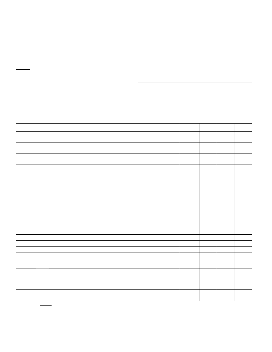
ABSOLUTE MAXIMUM RATINGS*
Supply Voltage (VCC to GND) ................................ +6.0V
RESET, RESET ............................ – 0.3V to (VCC + 0.3V)
Input Current, VCC.. .................................................. 20mA
Output Current, RESET, RESET ............................. 20mA
dV/dt (VCC) ....................................................... 100V/
sec
Operating Temperature Range ............. – 40
°C to +125°C
Power Dissipation (TA
≤ 70°C)
3-Pin SOT-23B (derate 4mW/
°C above +70°C) 230mW
3-Pin SC-70 (derate 2.17mW/
°C above +70°C) 174mW
Storage Temperature Range ................ – 65
°C to +150°C
Lead Temperature (Soldering, 10 sec) ................. +260
°C
*This is a stress rating only and functional operation of the device at these
or any other conditions above those indicated in the operational sections of
the specifications is not implied. Exposure to Absolute Maximum Rating
Conditions for extended periods may affect device reliability.
Symbol Parameter
Test Conditions
Min
Typ
Max
Unit
VCC Range
TA = 0
°C to +70°C
1.0
—
5.5
V
TA = – 40
°C to +125°C
1.2
—
5.5
ICC
Supply Current (SOT-23)
TCM8xxL/M/J VCC < 5.5V
—
24
60
A
TCM8xxR/S/T/Z: VCC < 3.6V
—
17
50
ICC
Supply Current (SC-70)
TCM8xxL/M/J VCC < 5.5V
—
16
35
A
TCM8xxR/S/T/Z: VCC < 3.6V
—
12
30
VTH
Reset Threshold (Note 2)
TCM8xxL: TA = +25
°C
4.56
4.63
4.70
V
TA = – 40
°C to +125°C
4.50
—
4.75
TCM8xxM: TA = +25
°C
4.31
4.38
4.45
TA = – 40
°C to +125°C
4.25
—
4.50
TCM809J: TA = +25
°C
3.93
4.00
4.06
TA = – 40
°C to +125°C
3.89
—
4.10
TCM8xxT: TA = +25
°C
3.04
3.08
3.11
TA = – 40
°C to +125°C
3.00
—
3.15
TCM8xxS: TA = +25
°C
2.89
2.93
2.96
TA = – 40
°C to +125°C
2.85
—
3.00
TCM8xxR: TA = +25
°C
2.59
2.63
2.66
TA = – 40
°C to +125°C
2.55
—
2.70
TCM8xxZ: TA = +25
°C
2.28
2.32
2.35
TA = – 40
°C to +125°C
2.25
—
2.38
Reset Threshold Tempco
—
30
—
ppm/
°C
VCC to Reset Delay (Note 2)
VCC = VTH to (VTH – 100mV)
—
20
—
sec
Reset Active Timeout Period
140
240
560
msec
VOL
RESET Output Voltage Low
TCM809R/S/T/Z: VCC = VTH min, ISINK = 1.2mA
—
0.3
V
(TCM809)
TCM809L/M/J: VCC = VTH min, ISINK = 3.2mA
—
0.4
VCC > 1.0V, ISINK = 50
A
—
0.3
VOH
RESET Output Voltage High
TCM809R/S/T/Z: VCC > VTH max, ISOURCE = 500
A 0.8 VCC
——
V
(TCM809)
TCM809L/M/J: VCC > VTH max, ISOURCE = 800
AVCC – 1.5
—
VOL
RESET Output Voltage Low
TCM810R/S/T/Z: VCC = VTH max, ISINK = 1.2mA
—
0.3
V
(TCM810)
TCM810L/M/J: VCC = VTH max, ISINK = 3.2mA
—
0.4
VOH
RESET Output Voltage High
1.8 < VCC < VTH min, ISOURCE = 150
A
0.8 VCC
——
V
(TCM810)
NOTES:
1. Production testing done at TA = +25
°C, over temperature limits by design.
2. RESET output for TCM809, RESET Output for TCM810.
ELECTRICAL CHARACTERISTICS:
Vcc = Full Range, TA = Operating Temperature Range unless other-
wise noted. Typical values are at TA = +25
°C, VCC = 5V for L/M/J, 3.3V for T/S, 3.0V for R, and 2.5V for Z (Note 1).
相關PDF資料 |
PDF描述 |
|---|---|
| TC54VC1601EMB | 1-CHANNEL POWER SUPPLY SUPPORT CKT, PSSO3 |
| TC54VC2002EMB | 1-CHANNEL POWER SUPPLY SUPPORT CKT, PSSO3 |
| TC54VC2702ECB | 1-CHANNEL POWER SUPPLY SUPPORT CKT, PDSO3 |
| TC54VC2902ECT | 1-CHANNEL POWER SUPPLY SUPPORT CKT, PDSO5 |
| TC54VC3601EMB | 1-CHANNEL POWER SUPPLY SUPPORT CKT, PSSO3 |
相關代理商/技術參數(shù) |
參數(shù)描述 |
|---|---|
| TCM809ZVB713 | 制造商:MICROCHIP 制造商全稱:Microchip Technology 功能描述:3-Pin Microcontroller Reset Monitors |
| TCM809ZVLB713 | 功能描述:監(jiān)控電路 Microprocessor 2.32V RoHS:否 制造商:STMicroelectronics 監(jiān)測電壓數(shù): 監(jiān)測電壓: 欠電壓閾值: 過電壓閾值: 輸出類型:Active Low, Open Drain 人工復位:Resettable 監(jiān)視器:No Watchdog 電池備用開關:No Backup 上電復位延遲(典型值):10 s 電源電壓-最大:5.5 V 最大工作溫度:+ 85 C 安裝風格:SMD/SMT 封裝 / 箱體:UDFN-6 封裝:Reel |
| TCM809ZVLB713 | 制造商:Microchip Technology Inc 功能描述:RESET MONITOR 2.32V SC-70-3 809 |
| TCM809ZVN | 制造商:MICROCHIP 制造商全稱:Microchip Technology 功能描述:3-Pin Microcontroller Reset Monitors |
| TCM809ZVNB713 | 功能描述:監(jiān)控電路 Microprocessor 2.32V RoHS:否 制造商:STMicroelectronics 監(jiān)測電壓數(shù): 監(jiān)測電壓: 欠電壓閾值: 過電壓閾值: 輸出類型:Active Low, Open Drain 人工復位:Resettable 監(jiān)視器:No Watchdog 電池備用開關:No Backup 上電復位延遲(典型值):10 s 電源電壓-最大:5.5 V 最大工作溫度:+ 85 C 安裝風格:SMD/SMT 封裝 / 箱體:UDFN-6 封裝:Reel |
發(fā)布緊急采購,3分鐘左右您將得到回復。