- 您現(xiàn)在的位置:買(mǎi)賣(mài)IC網(wǎng) > PDF目錄383935 > TCA7660 (Microchip Technology Inc.) HIGH FREQUENCY 7660 DC-TO-DC VOLTAGE CONVERTER PDF資料下載
參數(shù)資料
| 型號(hào): | TCA7660 |
| 廠商: | Microchip Technology Inc. |
| 英文描述: | HIGH FREQUENCY 7660 DC-TO-DC VOLTAGE CONVERTER |
| 中文描述: | 高頻7660型DC - DC電壓轉(zhuǎn)換器 |
| 文件頁(yè)數(shù): | 3/8頁(yè) |
| 文件大小: | 76K |
| 代理商: | TCA7660 |
3
HIGH FREQUENCY 7660 DC-TO-DC
VOLTAGE CONVERTER
TC7660H
TC7660H-2 10/1/96
2001 Microchip Technology Inc. DS21466A
Detailed Description
The TC7660H contains all the necessary circuitry to
implement a voltage inverter, with the exception of two
external capacitors, which may be inexpensive 1.0
μ
F
non-polarized capacitors. Operation is best understood by
considering Figure 2, which shows an idealized voltage
inverter. Capacitor C
1
is charged to a voltage, V
+
, for the half
cycle when switches S
1
and S
3
are closed. (Note:
Switches
S
2
and S
4
are open during this half cycle.) During the second
half cycle of operation, switches S
2
and S
4
are closed, with
S
1
and S
3
open, thereby shifting capacitor C
1
negatively by
V
+
volts. Charge is then transferred from C
1
to C
2
, such that
the voltage on C
2
is exactly V
+
, assuming ideal switches and
no load on C
2
.
V+
GND
S3
S1
S2
S4
C2
VOUT
=
–
VIN
Figure 2. Idealized Charge Pump Inverter
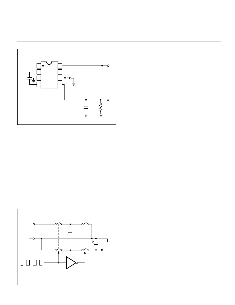
Figure 1. TC7660H Test Circuit
1
2
3
4
8
7
6
5
TC7660H
+
V+
(+5V)
C1
1.0
μ
F
+
C2
1.0
μ
F
RL
IS
To improve low-voltage operation, the LV pin should be
connected to GND. For supply voltages greater than 3.5V,
the LV terminal
must be left open to ensure latch-up-
proof operation and prevent device damage
.
Theoretical Power Efficiency Considerations
In theory, a capacitative charge pump can approach
100% efficiency if certain conditions are met:
(1) The drive circuitry consumes minimal power.
(2) The output switches have extremely low ON
resistance and virtually no offset.
(3) The impedances of the pump and reservoir
capacitors are negligible at the pump frequency.
The TC7660H approaches these conditions for nega-
tive voltage multiplication if large values of C
1
and C
2
are
used.
Energy is lost only in the transfer of charge
between capacitors if a change in voltage occurs.
The
energy lost is defined by:
E = 1/2 C
1
(V
12
– V
22
)
V
1
and V
2
are the voltages on C
1
during the pump and
transfer cycles. If the impedances of C
1
and C
2
are relatively
high at the pump frequency (refer to Figure 1), compared to
the value of R
L
, there will be a substantial difference in
voltages V
1
and V
2
. Therefore, it is not only desirable to
make C
2
as large as possible to eliminate output voltage
ripple, but also to employ a correspondingly large value for
C
1
in order to achieve maximum efficiency of operation.
Do's and Don'ts
Do not exceed maximum supply voltages.
Do not connect LV terminal to GND for supply voltages
greater than 3.5V.
Do not short circuit the output to V
+
supply for voltages
above 5.5V for extended periods; however, transient
conditions including start-up are okay.
When using polarized capacitors in the inverting mode,
the + terminal of C
1
must be connected to pin 2 of the
TC7660H and the + terminal of C
2
must be connected
to GND Pin 3.
相關(guān)PDF資料 |
PDF描述 |
|---|---|
| TCA785 | Phase Control IC |
| TCA785 | Phase Control IC |
| TCA830 | MONOLITHISH INTEGRIERTE SCHALTUNG MONOLITHIC INTEGRATED CIRCUIT |
| TCA830A | MONOLITHISH INTEGRIERTE SCHALTUNG MONOLITHIC INTEGRATED CIRCUIT |
| TCA965 | Window Discriminator(Bipolar IC) |
相關(guān)代理商/技術(shù)參數(shù) |
參數(shù)描述 |
|---|---|
| TCA771 | 制造商:INFINEON 制造商全稱(chēng):Infineon Technologies AG 功能描述:TRANSISTOR ARRAY WITH 5 NPN TRANSISTORS |
| TCA785 | 功能描述:接口 - 專(zhuān)用 Phase Control IC 8V-18V 10mA RoHS:否 制造商:Texas Instruments 產(chǎn)品類(lèi)型:1080p60 Image Sensor Receiver 工作電源電壓:1.8 V 電源電流:89 mA 最大功率耗散: 最大工作溫度:+ 85 C 安裝風(fēng)格:SMD/SMT 封裝 / 箱體:BGA-59 |
| TCA-785 | 制造商:Rochester Electronics LLC 功能描述: 制造商:Infineon Technologies AG 功能描述: |
| TCA785_05 | 制造商:INFINEON 制造商全稱(chēng):Infineon Technologies AG 功能描述:Phase Control IC |
| TCA785HKLA1 | 制造商:Infineon Technologies AG 功能描述:Phase Control IC 16-Pin PDIP 制造商:Infineon Technologies AG 功能描述:INDUSTRIAL IC - Rail/Tube 制造商:Infineon Technologies AG 功能描述:IC PHASE CONTROL 250MA OUT 16DIP |
發(fā)布緊急采購(gòu),3分鐘左右您將得到回復(fù)。