- 您現(xiàn)在的位置:買賣IC網(wǎng) > PDF目錄9453 > TC530COI (Microchip Technology)IC DATA ACQ SUBSYSTEM 28SOIC PDF資料下載
參數(shù)資料
| 型號: | TC530COI |
| 廠商: | Microchip Technology |
| 文件頁數(shù): | 8/28頁 |
| 文件大小: | 0K |
| 描述: | IC DATA ACQ SUBSYSTEM 28SOIC |
| 標(biāo)準(zhǔn)包裝: | 27 |
| 類型: | 數(shù)據(jù)采集系統(tǒng)(DAS) |
| 分辨率(位): | 17 b |
| 采樣率(每秒): | 6.5 |
| 數(shù)據(jù)接口: | 串行 |
| 電壓電源: | 單電源 |
| 電源電壓: | 4.5 V ~ 5.5 V |
| 工作溫度: | 0°C ~ 70°C |
| 安裝類型: | 表面貼裝 |
| 封裝/外殼: | 28-SOIC(0.295",7.50mm 寬) |
| 供應(yīng)商設(shè)備封裝: | 28-SOIC |
| 包裝: | 管件 |
第1頁第2頁第3頁第4頁第5頁第6頁第7頁當(dāng)前第8頁第9頁第10頁第11頁第12頁第13頁第14頁第15頁第16頁第17頁第18頁第19頁第20頁第21頁第22頁第23頁第24頁第25頁第26頁第27頁第28頁
TC530/TC534
DS21433C-page 16
2007 Microchip Technology Inc.
6.4
Data Read Cycle
Data is shifted out of the serial port in the following
order: End of Conversion (EOC), Overrange (OVR),
Polarity (POL), conversion data (MSB first). When R/W
is high, the state of the EOC bit can be polled by simply
reading the state of DOUT. This allows the processor to
determine if new data is available without connecting
an additional wire to the EOC output pin (this is
especially useful in a polled environment). Refer to
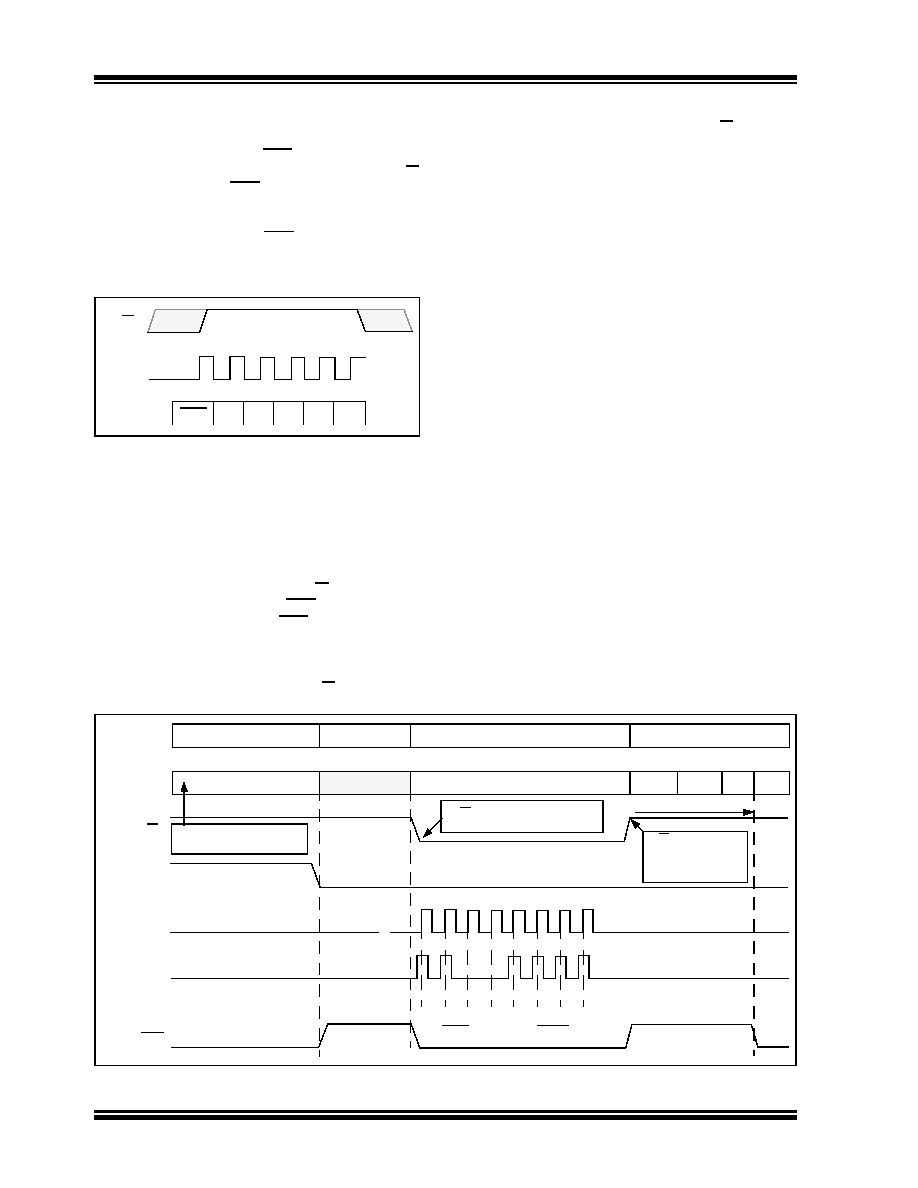
FIGURE 6-1:
Serial Port Data Read
Cycle.
6.5
Load Value Write Cycle
Following the power-up reset pulse, the LOAD VALUE
(which sets the duration of AZ and INT) must next be
transmitted to the serial port. To accomplish this, the
processor monitors the state of EOC (which is available
as a hardware output or at DOUT). R/W is taken low to
initiate the write cycle only when EOC is low (during the
AZ phase). (Failure to observe EOC low may cause an
offset voltage to be developed across CINT, resulting in
erroneous readings). The 8-bit LOAD VALUE data on
DIN is clocked in by DCLK. The processor then
terminates the write cycle by taking R/W high. (Data is
transferred from the serial input shift register to the time
base counter on the rising edge of R/W and data
conversion is initiated). See Figure 6-2.
6.6
Input Multiplexer (TC534 Only)
A 4-input, differential multiplexer is included in the
TC534. The states of channel address lines A0 and A1
determine which differential VIN pair is routed to the
converter input. A0 is the least significant address bit
(i.e., channel 1 is selected when A0 = 0 and A1 = 0).
The multiplexer is designed to be operated in a differ-
ential mode. For single-ended inputs, the CHx- input for
the channel under selection must be connected to the
ground reference associated with the input signal.
6.7
DC/DC Converter
An on-board, TC7660H-type charge pump supplies
negative bias to the converter circuitry, as well as to
external devices. The charge pump develops a
negative output voltage by moving charge from the
power supply to the reservoir capacitor at VSS by way
of the commutating capacitor connected to the CAP+
and CAP- inputs.
The charge pump clock operates at a typical frequency
of 100 kHz. If lower quiescent current is desired, the
charge pump clock can be slowed by connecting an
external capacitor from the OSC pin to VDD. Reference
typical characteristics curves.
FIGURE 6-2:
TC530/TC534 Initialization and Load Value Write Cycle.
EOC OVR POL MSB
LSB
R/W
DCLK
DOUT
EOC
R/W
RESET
DCLK
DIN
1
00
11
1
AZ
LOAD VALUE
MSB
LSB
INT
DINT
IZ
AZ...
Conversion
Phase
Timing
Status
Converter held in AZ
state due to RESET =
1
Write LOAD VALUE to Serial Port
Power-up RESET
Undefined
Converter in Normal Service
R/W brought LOW during AZ
for serial port write cycle
R/W = HIGH strobes
LOAD VALUE into
timebase and starts
conversion
Continuous Conversions
相關(guān)PDF資料 |
PDF描述 |
|---|---|
| TC534CKW | IC DATA ACQ SUBSYSTEM 44-MQFP |
| MS27497T22A21S | CONN RCPT 21POS WALL MNT W/SCKT |
| TC534CPL | IC DATA ACQ SUBSYSTEM 40DIP |
| MS27473T22A1PD | CONN PLUG 100POS STRAIGHT W/PINS |
| TC530CPJ | IC DATA ACQ SUBSYSTEM 28DIP |
相關(guān)代理商/技術(shù)參數(shù) |
參數(shù)描述 |
|---|---|
| TC530COI713 | 功能描述:數(shù)據(jù)轉(zhuǎn)換系統(tǒng) Prec Data Acq Subsys RoHS:否 制造商:Texas Instruments 轉(zhuǎn)換速率:0.001 MSPs 分辨率:24 bit 最大工作溫度:+ 125 C 最小工作溫度:- 40 C 安裝風(fēng)格:SMD/SMT 封裝 / 箱體:TQFP-64 封裝:Reel |
| TC530CPJ | 功能描述:數(shù)據(jù)轉(zhuǎn)換系統(tǒng) Prec Data Acq Subsys RoHS:否 制造商:Texas Instruments 轉(zhuǎn)換速率:0.001 MSPs 分辨率:24 bit 最大工作溫度:+ 125 C 最小工作溫度:- 40 C 安裝風(fēng)格:SMD/SMT 封裝 / 箱體:TQFP-64 封裝:Reel |
| TC531000AP-F711 | 制造商:Toshiba America Electronic Components 功能描述:531000AP-F711 |
| TC531001 | 制造商:TOSHIBA 制造商全稱:Toshiba Semiconductor 功能描述:1M BIT (128K WORD x 8 BIT) CMOS MASK ROM |
| TC531001CF | 制造商:Toshiba America Electronic Components 功能描述: |
發(fā)布緊急采購,3分鐘左右您將得到回復(fù)。