- 您現(xiàn)在的位置:買賣IC網(wǎng) > PDF目錄383888 > TC1302BDTVUATR (Microchip Technology Inc.) LOW QUIESCENT CURRENT DUAL OUTPUT LDO PDF資料下載
參數(shù)資料
| 型號: | TC1302BDTVUATR |
| 廠商: | Microchip Technology Inc. |
| 元件分類: | 基準電壓源/電流源 |
| 英文描述: | LOW QUIESCENT CURRENT DUAL OUTPUT LDO |
| 中文描述: | 低靜態(tài)電流雙輸出穩(wěn)壓器 |
| 文件頁數(shù): | 11/26頁 |
| 文件大小: | 570K |
| 代理商: | TC1302BDTVUATR |
2005 Microchip Technology Inc.
DS21333B-page 11
TC1302A/B
4.0
TC1302B PIN DESCRIPTIONS
The descriptions of the pins are listed in Table 4-1.
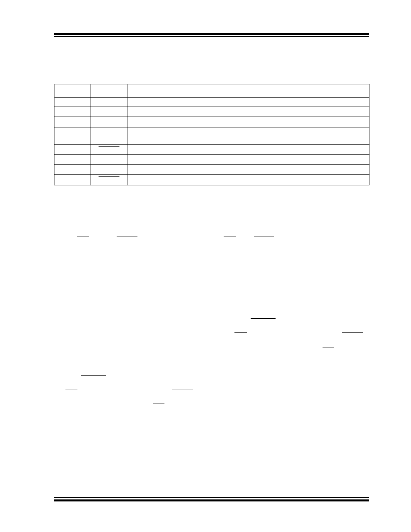
TABLE 4-1:
TC1302B PIN FUNCTION TABLE
4.1
Regulated Output Voltage #1
(V
OUT1
)
Connect V
OUT1
to the positive side of the V
OUT1
capacitor and load. Capable of 300 mA maximum
output current. For the TC1302B, V
OUT1
can be turned
ON and OFF using the SHDN1 input pin.
4.2
Circuit Ground Pin (GND)
Connect GND to the negative side of the input and
output capacitor. Only the LDO internal circuitry bias
current flows out of this pin (200 μA maximum).
4.3
Reference Bypass Input
By connecting an external 10 nF capacitor (typical) to
the bypass input, both outputs (V
OUT1
and V
OUT2
) will
have less noise and improved Power Supply Ripple
Rejection (PSRR) performance. The LDO output
voltage startup time will increase with the addition of an
external bypass capacitor. By leaving this pin
unconnected, the startup time will be minimized.
4.4
Output Voltage #2 Shutdown
(SHDN2)
ON/OFF control is performed by connecting SHDN2 to
its proper level. When this pin is connected to a voltage
less than 15% of V
IN
, V
OUT2
will be OFF. If this pin is
connected to a voltage that is greater than 45% of V
IN
,
V
OUT2
will be turned ON.
4.5
Regulated Output Voltage #2
(V
OUT2
)
Connect V
OUT2
to the positive side of the V
OUT2
capacitor and load. This pin is capable of a maximum
output current of 150 mA. V
OUT2
can be turned ON and
OFF using SHDN2.
4.6
Unregulated Input Voltage Pin
(V
IN
)
Connect the unregulated input voltage source to V
IN
. If
the input voltage source is located more than several
inches away, or is a battery, a typical minimum input
capacitance of 1 μF and 4.7 μF is recommended.
4.7
Output Voltage #1 Shutdown
(SHDN1)
ON/OFF control is performed by connecting SNDN1 to
its proper level. When this pin is connected to a voltage
less than 15% of V
IN
, V
OUT1
will be OFF. If this pin is
connected to a voltage that is greater than 45% of V
IN
,
V
OUT1
will be turned ON.
Pin No.
Name
Function
1
2
3
4
NC
V
OUT1
GND
Bypass
No connect.
Regulated output voltage #1, capable of 300 mA.
Circuit ground pin.
Internal reference bypass pin. A 10 nF external capacitor can be used to further reduce
output noise and improve PSRR performance.
Output #2 shutdown control input.
Regulated output voltage #2, capable of 150 mA.
Unregulated Input voltage pin.
Output #1 shutdown control input.
5
6
7
8
SHDN2
V
OUT2
V
IN
SHDN1
相關(guān)PDF資料 |
PDF描述 |
|---|---|
| TC1302BIPVUATR | LOW QUIESCENT CURRENT DUAL OUTPUT LDO |
| TC1303A-AK3EUN | 500 mA Synchronous Buck Regulator, + 300 mA LDO with Power-Good Output |
| TC1303A-AB2EMFTR | 500 mA Synchronous Buck Regulator, + 300 mA LDO with Power-Good Output |
| TC1303A-AB2EUN | 500 mA Synchronous Buck Regulator, + 300 mA LDO with Power-Good Output |
| TC1303A-AB2EUNTR | 500 mA Synchronous Buck Regulator, + 300 mA LDO with Power-Good Output |
相關(guān)代理商/技術(shù)參數(shù) |
參數(shù)描述 |
|---|---|
| TC1302B-DTVUATR | 功能描述:低壓差穩(wěn)壓器 - LDO Dual CMOS LDO 300mA & 150mA RoHS:否 制造商:Texas Instruments 最大輸入電壓:36 V 輸出電壓:1.4 V to 20.5 V 回動電壓(最大值):307 mV 輸出電流:1 A 負載調(diào)節(jié):0.3 % 輸出端數(shù)量: 輸出類型:Fixed 最大工作溫度:+ 125 C 安裝風(fēng)格:SMD/SMT 封裝 / 箱體:VQFN-20 |
| TC1302BHPVMF | 制造商:MICROCHIP 制造商全稱:Microchip Technology 功能描述:LOW QUIESCENT CURRENT DUAL OUTPUT LDO |
| TC1302B-HPVMF | 功能描述:低壓差穩(wěn)壓器 - LDO Dual CMOS LDO 300mA & 150mA RoHS:否 制造商:Texas Instruments 最大輸入電壓:36 V 輸出電壓:1.4 V to 20.5 V 回動電壓(最大值):307 mV 輸出電流:1 A 負載調(diào)節(jié):0.3 % 輸出端數(shù)量: 輸出類型:Fixed 最大工作溫度:+ 125 C 安裝風(fēng)格:SMD/SMT 封裝 / 箱體:VQFN-20 |
| TC1302BHPVMFTR | 制造商:MICROCHIP 制造商全稱:Microchip Technology 功能描述:LOW QUIESCENT CURRENT DUAL OUTPUT LDO |
| TC1302B-HPVMFTR | 功能描述:低壓差穩(wěn)壓器 - LDO Dual CMOS LDO 300mA & 150mA RoHS:否 制造商:Texas Instruments 最大輸入電壓:36 V 輸出電壓:1.4 V to 20.5 V 回動電壓(最大值):307 mV 輸出電流:1 A 負載調(diào)節(jié):0.3 % 輸出端數(shù)量: 輸出類型:Fixed 最大工作溫度:+ 125 C 安裝風(fēng)格:SMD/SMT 封裝 / 箱體:VQFN-20 |
發(fā)布緊急采購,3分鐘左右您將得到回復(fù)。