- 您現(xiàn)在的位置:買賣IC網(wǎng) > PDF目錄383888 > TC1302A (Microchip Technology Inc.) LOW QUIESCENT CURRENT DUAL OUTPUT LDO PDF資料下載
參數(shù)資料
| 型號: | TC1302A |
| 廠商: | Microchip Technology Inc. |
| 元件分類: | 基準(zhǔn)電壓源/電流源 |
| 英文描述: | LOW QUIESCENT CURRENT DUAL OUTPUT LDO |
| 中文描述: | 低靜態(tài)電流雙輸出穩(wěn)壓器 |
| 文件頁數(shù): | 4/26頁 |
| 文件大小: | 570K |
| 代理商: | TC1302A |
第1頁第2頁第3頁當(dāng)前第4頁第5頁第6頁第7頁第8頁第9頁第10頁第11頁第12頁第13頁第14頁第15頁第16頁第17頁第18頁第19頁第20頁第21頁第22頁第23頁第24頁第25頁第26頁
TC1302A/B
DS21333B-page 4
2005 Microchip Technology Inc.
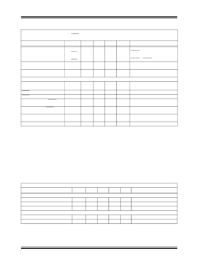
TEMPERATURE SPECIFICATIONS
Shutdown Supply Current
TC1302A
Shutdown Supply Current
TC1302B
Power Supply Rejection Ratio
I
IN_SHDNA
—
58
90
μA
SHDN2 = GND
I
IN_SHDNB
PSRR
—
—
0.1
58
1
—
μA
dB
SHDN1 = SHDN2 = GND
f
≤
100 Hz, I
OUT1
= I
OUT2
= 50 mA,
C
IN
= 0 μF
f
≤
1 kHz, I
OUT1
= I
OUT2
= 50 mA,
C
IN
= 0 μF
Output Noise
eN
—
830
—
nV/(Hz)
Output Short Circuit Current (Average)
V
OUT1
V
OUT2
SHDN Input High Threshold
SHDN Input Low Threshold
Wake Up Time (From SHDN
mode), (V
OUT2
)
Settling Time (From SHDN mode),
(V
OUT2
)
Thermal Shutdown Die
Temperature
Thermal Shutdown Hysteresis
Note
1:
The minimum V
IN
has to meet two conditions: V
IN
≥
2.7V and V
IN
≥
V
R
+ V
DROPOUT
.
2:
V
R
is defined as the higher of the two regulator nominal output voltages (V
OUT1
or V
OUT2
).
3:
TCV
OUT
= ((V
OUTmax
- V
OUTmin
) * 10
6
)/(V
OUT
*
Δ
T).
4:
Regulation is measured at a constant junction temperature using low duty-cycle pulse testing. Load regulation is tested
over a load range from 0.1 mA to the maximum specified output current. Changes in output voltage due to heating
effects are covered by the thermal regulation specification.
5:
Thermal regulation is defined as the change in output voltage at a time t after a change in power dissipation is applied,
excluding load or line regulation effects. Specifications are for a current pulse equal to I
LMAX
at V
IN
= 6V for t = 10 msec.
6:
Dropout voltage is defined as the input-to-output voltage differential at which the output voltage drops 2% below its
value measured at a 1V differential.
7:
The maximum allowable power dissipation is a function of ambient temperature, the maximum allowable junction
temperature and the thermal resistance from junction to air (i.e., T
A
, T
J
,
θ
JA
). Exceeding the maximum allowable power
dissipation causes the device to initiate thermal shutdown.
I
OUTsc1
I
OUTsc2
V
IH
V
IL
t
WK
—
—
45
—
—
200
140
—
—
5.3
—
—
—
15
20
mA
mA
%V
IN
%V
IN
μs
R
LOAD1
≤
1
Ω
R
LOAD2
≤
1
Ω
V
IN
= 2.7V to 6.0V
V
IN
= 2.7V to 6.0V
V
IN
= 5V, I
OUT1
= I
OUT2
= 30 mA,
See Figure 5-1
V
IN
= 5V, I
OUT1
= I
OUT2
= 50 mA,
See Figure 5-2
V
IN
= 5V, I
OUT1
= I
OUT2
= 100 μA
t
S
—
50
—
μs
T
SD
—
150
—
°C
T
HYS
—
10
—
°C
V
IN
= 5V
Electrical Specifications:
Unless otherwise indicated, all limits are specified for: V
IN
= +2.7V to +6.0V.
Parameters
Sym
Min
Typ
Max
Units
Conditions
Temperature Ranges
Operating Junction Temperature Range
Storage Temperature Range
Maximum Junction Temperature
Thermal Package Resistances
Thermal Resistance, MSOP8
Thermal Resistance, DFN8
T
A
T
A
T
J
-40
-65
—
—
—
—
+125
+150
+150
°C
°C
°C
Steady State
Transient
θ
JA
θ
JA
—
—
208
41
—
—
°C/W
°C/W
Typical 4-Layer Board
Typical 4-Layer Board with Vias
DC CHARACTERISTICS (Continued)
Electrical Specifications:
Unless otherwise noted, V
IN
= V
R
+1V, I
OUT1
=
I
OUT2
= 100 μA, C
IN
= 4.7 μF,
C
OUT1
= C
OUT2
= 1 μF, C
BYPASS
= 10 nF, SHDN > V
IH
, T
A
= +25°C.
Boldface
type specifications apply for junction temperatures of -40°C to +125°C.
Parameters
Sym
Min
Typ
Max
Units
Conditions
相關(guān)PDF資料 |
PDF描述 |
|---|---|
| TC1302ADTVMF | LOW QUIESCENT CURRENT DUAL OUTPUT LDO |
| TC1302BIPVMF | LOW QUIESCENT CURRENT DUAL OUTPUT LDO |
| TC1302BIPVMFTR | LOW QUIESCENT CURRENT DUAL OUTPUT LDO |
| TC1302BIPVUA | LOW QUIESCENT CURRENT DUAL OUTPUT LDO |
| TC1302ADTVMFTR | LOW QUIESCENT CURRENT DUAL OUTPUT LDO |
相關(guān)代理商/技術(shù)參數(shù) |
參數(shù)描述 |
|---|---|
| TC1302A_13 | 制造商:MICROCHIP 制造商全稱:Microchip Technology 功能描述:Low Quiescent Current Dual Output LDO |
| TC1302ADTVMF | 制造商:MICROCHIP 制造商全稱:Microchip Technology 功能描述:LOW QUIESCENT CURRENT DUAL OUTPUT LDO |
| TC1302A-DTVMF | 功能描述:低壓差穩(wěn)壓器 - LDO Dual CMOS LDO 300mA & 150mA RoHS:否 制造商:Texas Instruments 最大輸入電壓:36 V 輸出電壓:1.4 V to 20.5 V 回動電壓(最大值):307 mV 輸出電流:1 A 負(fù)載調(diào)節(jié):0.3 % 輸出端數(shù)量: 輸出類型:Fixed 最大工作溫度:+ 125 C 安裝風(fēng)格:SMD/SMT 封裝 / 箱體:VQFN-20 |
| TC1302ADTVMFTR | 制造商:MICROCHIP 制造商全稱:Microchip Technology 功能描述:LOW QUIESCENT CURRENT DUAL OUTPUT LDO |
| TC1302A-DTVMFTR | 功能描述:低壓差穩(wěn)壓器 - LDO Dual CMOS LDO 300mA & 150mA RoHS:否 制造商:Texas Instruments 最大輸入電壓:36 V 輸出電壓:1.4 V to 20.5 V 回動電壓(最大值):307 mV 輸出電流:1 A 負(fù)載調(diào)節(jié):0.3 % 輸出端數(shù)量: 輸出類型:Fixed 最大工作溫度:+ 125 C 安裝風(fēng)格:SMD/SMT 封裝 / 箱體:VQFN-20 |
發(fā)布緊急采購,3分鐘左右您將得到回復(fù)。