- 您現(xiàn)在的位置:買(mǎi)賣(mài)IC網(wǎng) > PDF目錄383883 > TC1269-30VUA (Microchip Technology Inc.) 300mA CMOS LDO with Shutdown and VREF Bypass PDF資料下載
參數(shù)資料
| 型號(hào): | TC1269-30VUA |
| 廠商: | Microchip Technology Inc. |
| 英文描述: | 300mA CMOS LDO with Shutdown and VREF Bypass |
| 中文描述: | 300mA的CMOS LDO穩(wěn)壓器具有關(guān)斷和VREF繞道 |
| 文件頁(yè)數(shù): | 2/12頁(yè) |
| 文件大小: | 432K |
| 代理商: | TC1269-30VUA |
TC1269
DS21380B-page 2
2002 Microchip Technology Inc.
1.0
ELECTRICAL
CHARACTERISTICS
Absolute Maximum Ratings*
Input Voltage .........................................................6.5V
Output Voltage.................... (V
SS
– 0.3) to (V
IN
+ 0.3V)
Maximum Voltage on Any Pin ........V
IN
+0.3V to -0.3V
Power Dissipation................Internally Limited
(Note 6)
Operating Temperature ...............-40°C < T
J
< +125°C
Storage Temperature..........................-65°C to +150°C
*Stresses above those listed under "Absolute Maximum
Ratings" may cause permanent damage to the device. These
are stress ratings only and functional operation of the device
at these or any other conditions above those indicated in the
operation sections of the specifications is not implied.
Exposure to Absolute Maximum Rating conditions for
extended periods may affect device reliability.
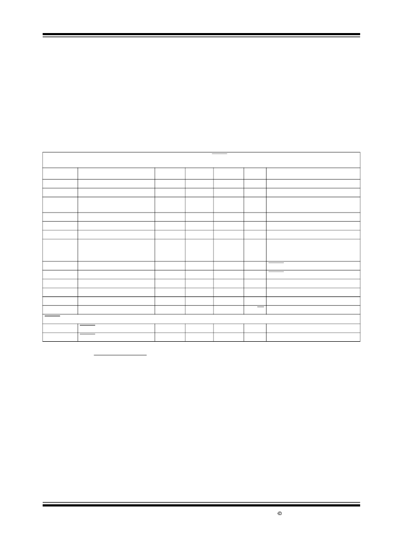
TC1269 ELECTRICAL SPECIFICATIONS
Electrical Characteristics:
V
IN
= V
OUT
+ 1V, I
L
= 0.1
μ
A, C
L
= 3.3
μ
F, SHDN > V
IH
, T
A
= 25°C, unless otherwise noted.
Boldface
type specifications apply for junction temperatures of -40°C to +125°C.
Symbol
Parameter
Min
Typ
Max
Units
Test Conditions
V
IN
I
OUT
MAX
V
OUT
Input Operating Voltage
Maximum Output Current
Output Voltage
—
300
—
—
—
6.0
—
—
V
mA
V
V
R
– 2.5%
—
—
—
—
—
—
—
—
—
—
—
—
V
R
±0.5%
—
40
0.05
0.5
20
80
240
50
0.05
50
550
0.04
260
V
R
+ 2.5%
—
0.35
2.0
30
160
480
90
0.5
—
650
—
—
Note 1
V
OUT
/
T
V
OUT
/
V
IN
V
OUT
/V
OUT
V
IN
-V
OUT
V
OUT
Temperature Coefficient
Line Regulation
Load Regulation
Dropout Voltage
ppm/°C
Note 2
%
%
mV
(V
R
+ 1V)
≤
V
IN
≤
6V
I
L
= 0.1mA to I
OUT
MAX
I
L
= 0.1mA
I
L
= 100mA
I
L
= 300mA
(Note 4)
SHDN = V
IH
SHDN = 0V
F
RE
≤
120Hz
V
OUT
= 0V
Note 5
nV/
√
Hz F = 1kHz, C
OUT
= 1
μ
F, R
LOAD
= 50
I
SS1
I
SS2
PSRR
I
OUTSC
V
OUT
/
P
D
eN
Supply Current
Shutdown Supply Current
Power Supply Rejection Ratio
Output Short Circuit Current
Thermal Regulation
Output Noise
μ
A
μ
A
dB
mA
V/W
SHDN Input
V
IH
V
IL
Note 1:
2:
SHDN Input High Threshold
SHDN Input Low Threshold
45
—
—
—
—
15
%V
IN
%V
IN
V
R
is the regulator output voltage setting.
T
C
V
OUT
= (V
OUT
MAX
– V
OUT
MIN
) x 10
V
OUT
x
T
3:
Regulation is measured at a constant junction temperature using low duty cycle pulse testing. Load regulation is tested over a load range from
0.1mA to the maximum specified output current. Changes in output voltage due to heating effects are covered by the thermal regulation specifica-
tion.
Dropout voltage is defined as the input to output differential at which the output voltage drops2% below its nominal value measured at a 1V differen-
tial.
Thermal Regulation is defined as the change in output voltage at a time T after a change in power dissipation is applied, excluding load or
line regulation effects. Specifications are for a current pulse equal to I
at V
= 6V for T = 10 msec.
The maximum allowable power dissipation is a function of ambient temperature, the maximum allowable junction temperature and the
thermal resistance from junction-to-air (i.e., T
, T
,
θ
). Exceeding the maximum allowable power dissipation causes the device to initiate
thermal shutdown. Please see Section 4.0 Thermal Considerations for more details.
4:
5:
6:
相關(guān)PDF資料 |
PDF描述 |
|---|---|
| TC1269-50VUA | 300mA CMOS LDO with Shutdown and VREF Bypass |
| TC1269-33VUA | 300mA CMOS LDO with Shutdown and VREF Bypass |
| TC1269-28VUA | 300mA CMOS LDO with Shutdown and VREF Bypass |
| TC1270A | Voltage Supervisor with Manual Reset Input |
| TC1270ALBVCTTR | Voltage Supervisor with Manual Reset Input |
相關(guān)代理商/技術(shù)參數(shù) |
參數(shù)描述 |
|---|---|
| TC1269-33VUA | 制造商:MICROCHIP 制造商全稱(chēng):Microchip Technology 功能描述:300mA CMOS LDO with Shutdown and VREF Bypass |
| TC1269-5.0VUA | 功能描述:低壓差穩(wěn)壓器 - LDO 300mA Adj LDO RoHS:否 制造商:Texas Instruments 最大輸入電壓:36 V 輸出電壓:1.4 V to 20.5 V 回動(dòng)電壓(最大值):307 mV 輸出電流:1 A 負(fù)載調(diào)節(jié):0.3 % 輸出端數(shù)量: 輸出類(lèi)型:Fixed 最大工作溫度:+ 125 C 安裝風(fēng)格:SMD/SMT 封裝 / 箱體:VQFN-20 |
| TC1269-5.0VUATR | 功能描述:低壓差穩(wěn)壓器 - LDO 300mA Adj LDO RoHS:否 制造商:Texas Instruments 最大輸入電壓:36 V 輸出電壓:1.4 V to 20.5 V 回動(dòng)電壓(最大值):307 mV 輸出電流:1 A 負(fù)載調(diào)節(jié):0.3 % 輸出端數(shù)量: 輸出類(lèi)型:Fixed 最大工作溫度:+ 125 C 安裝風(fēng)格:SMD/SMT 封裝 / 箱體:VQFN-20 |
| TC1269-50VUA | 制造商:MICROCHIP 制造商全稱(chēng):Microchip Technology 功能描述:300mA CMOS LDO with Shutdown and VREF Bypass |
| TC126A | 制造商:Thomas & Betts 功能描述:Fittings Connector 2inch Steel |
發(fā)布緊急采購(gòu),3分鐘左右您將得到回復(fù)。