- 您現(xiàn)在的位置:買賣IC網(wǎng) > PDF目錄383882 > TC120 (Microchip Technology Inc.) PWM/PFM Step-Down Combination Regulator/Controller PDF資料下載
參數(shù)資料
| 型號(hào): | TC120 |
| 廠商: | Microchip Technology Inc. |
| 英文描述: | PWM/PFM Step-Down Combination Regulator/Controller |
| 中文描述: | PWM / PFM切換降壓組合穩(wěn)壓器/控制器 |
| 文件頁數(shù): | 2/14頁 |
| 文件大小: | 436K |
| 代理商: | TC120 |
TC120
DS21365B-page 2
2002 Microchip Technology Inc.
1.0
ELECTRICAL
CHARACTERISTICS
Absolute Maximum Ratings*
Power Supply Voltage (V
IN
)....................-0.3V to +12V
Voltage on V
OUT
Pin...............................-0.3V to +12V
Voltage on LX, Boost Pins
................................... (V
IN
– 12V) to (V
IN
+ 0.3V)
Voltage on EXT1, EXT2, SHDN Pins
.......................................... (-0.3V) to (V
IN
+ 0.3V)
L
X
Pin Current ..............................................700mA pk
EXT1, EXT2 Pin Current...................................±50mA
Continuous Power Dissipation .........................300mW
Operating Temperature Range.............-40°C to +85°C
Storage Temperature Range..............-40°C to +150°C
*Stresses above those listed under "Absolute Maximum
Ratings" may cause permanent damage to the device. These
are stress ratings only and functional operation of the device
at these or any other conditions above those indicated in the
operation sections of the specifications is not implied.
Exposure to Absolute Maximum Rating conditions for
extended periods may affect device reliability.
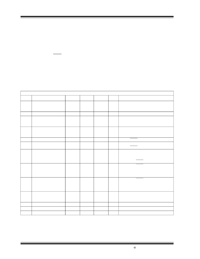
TC120 ELECTRICAL SPECIFICATIONS
Electrical Characteristics:
Test circuit of Figure 3-1, T
A
= 25
°
C, V
IN
= V
R
x 1.2, Note 1 unless otherwise noted.
Symbol
Parameter
Min
Typ
Max
Units
Test Conditions
V
OUT
Output Voltage
V
R
x 0.975 V
R
± 0.5% V
R
x 1.025
V
V
OUT
= 3.0V
V
OUT
= 3.3V
V
OUT
= 5.0V
I
OUT
= 120mA (Note 1)
I
OUT
= 132mA
I
OUT
= 200mA
V
IN
I
OUT
MAX
Input Voltage
Maximum Output Current
1.8
500
600
600
—
—
—
—
—
52
55
71
1.5
—
1.5
0.69
0.64
0.44
10.0
—
—
—
82
86
110
2.5
2
2.5
0.94
0.85
0.58
V
mA
V
OUT
= 3.0V
V
OUT
= 3.3V
V
OUT
= 5.0V
V
OUT
= 3.0V
V
OUT
= 3.3V
V
OUT
= 5.0V
No load, SHDN = 0V, (Note 2)
Measured at EXT1 Pin (Note 2)
No load, SHDN = 0V
V
OUT
= 3.0V
V
OUT
= 3.3V
V
OUT
= 5.0V
Resistor from L
X
to V
IN
,
SHDN = V
IN
V
OUT
= 3.0V
V
OUT
= 3.3V
V
OUT
= 5.0V
V
EXT1
= V
EXT2
= (V
IN
– 0.4V);
V
OUT
= V
IN
(Note 2)
V
OUT
= 3.0V
V
OUT
= 3.3V
V
OUT
= 5.0V
resistance of 200
to a voltage
such that VEXT1, 2 = 0.4V
Measured at EXT1 Pin,
V
IN
= V
OUT
+ 0.3V,
I
OUT
= 20mA (Note 3)
I
IN
Supply Current
μ
A
V
IN
= V
R
x 1.05, no load
I
SHDN
I
LX
Shutdown Supply Current
LX Pin Leakage Current
—
—
—
—
—
—
μ
A
μ
A
R
DSON
(
L
X
)
LX Pin ON Resistance
V
OUT
= V
R
x 0.9 (Note 2)
V
LX
= V
IN
– 0.2V, 10
R
EXTH
EXT1, EXT2
On Resistance to V
IN
—
—
—
38
35
24
52
47
32
SHDN = V
IH
; EXT1 and EXT2
connected to 200
load,
R
EXTL
EXT1, EXT2
On Resistance to GND
—
—
—
31
29
20
41
37
26
SHDN = V
IH
; EXT1 and EXT2
pulled up through a series
f
OSC
Oscillator Frequency
255
300
345
kHz
D
PWM
D
PFM
η
Maximum PWM Duty Cycle
PFM Duty Cycle
Efficiency
—
15
—
—
25
95
100
35
—
%
%
%
No load
V
IN
> V
R
x 1.2
Note
1:
2:
3:
V
is the factory-programmed output voltage setting.
No external components connected, except C
SS.
While operating in PWM Mode.
相關(guān)PDF資料 |
PDF描述 |
|---|---|
| TC120333EHA | PWM/PFM Step-Down Combination Regulator/Controller |
| TC120503EHA | PWM/PFM Step-Down Combination Regulator/Controller |
| TC1223 | 50mA and 100mA CMOS LDOs with Shutdown |
| TC1223-XXVCT | 50mA and 100mA CMOS LDOs with Shutdown |
| TC1224-XXVCT | 50mA and 100mA CMOS LDOs with Shutdown |
相關(guān)代理商/技術(shù)參數(shù) |
參數(shù)描述 |
|---|---|
| TC-120 | 制造商:PROTECTIVE CLOSURES 功能描述: |
| TC-120.000MBD-T | 功能描述:標(biāo)準(zhǔn)時(shí)鐘振蕩器 120.000MHz 3.3V 25ppm -40C to 85C RoHS:否 制造商:AVX 產(chǎn)品:Standard Clock Oscillators 封裝 / 箱體:7 mm x 5 mm 頻率:75 MHz 頻率穩(wěn)定性:50 PPM 電源電壓:2.5 V 負(fù)載電容: 端接類型:SMD/SMT 最小工作溫度:0 C 最大工作溫度:+ 70 C 輸出格式:LVDS 尺寸: 封裝:Reel 系列: |
| TC-120.000MBE-T | 制造商:TXC Corporation 功能描述:OSC MEMS 120.000 MHZ 3.3V SMD |
| TC-120.000MCD-T | 功能描述:標(biāo)準(zhǔn)時(shí)鐘振蕩器 120.000MHz 2.5V 25ppm -40C to 85C RoHS:否 制造商:AVX 產(chǎn)品:Standard Clock Oscillators 封裝 / 箱體:7 mm x 5 mm 頻率:75 MHz 頻率穩(wěn)定性:50 PPM 電源電壓:2.5 V 負(fù)載電容: 端接類型:SMD/SMT 最小工作溫度:0 C 最大工作溫度:+ 70 C 輸出格式:LVDS 尺寸: 封裝:Reel 系列: |
| TC-120.000MCE-T | 制造商:TXC Corporation 功能描述:OSC MEMS 120.000 MHZ 2.5V SMD |
發(fā)布緊急采購,3分鐘左右您將得到回復(fù)。