- 您現(xiàn)在的位置:買賣IC網(wǎng) > PDF目錄383878 > TAS5100ADAPR (Texas Instruments, Inc.) Single Audio Amplifier PDF資料下載
參數(shù)資料
| 型號: | TAS5100ADAPR |
| 廠商: | Texas Instruments, Inc. |
| 元件分類: | 運(yùn)動控制電子 |
| 英文描述: | Single Audio Amplifier |
| 中文描述: | 單音頻放大器 |
| 文件頁數(shù): | 5/16頁 |
| 文件大小: | 214K |
| 代理商: | TAS5100ADAPR |
TAS5100A
SLES030
–
FEBRUARY 2002
5
www.ti.com
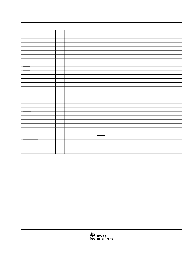
Terminal Functions
TERMINAL
NAME
BIAS_A
BIAS_B
BOOTSTRAPA
BOOTSTRAPB
DVDD
DVSS
I/O
DESCRIPTION
NO.
11
12
30
19
6
7, 8, 9
I
I
Connect external resistor to DVSS. See application note SLAA117
Connect external resistor to DVSS. See application note SLAA117
Bootstrap capacitor pin for H-bridge A
Bootstrap capacitor pin for H-bridge B
3.3-V digital voltage supply for logic
Digital ground for logic is internally connected to PVSS. All three pins must be tied together but not
connected externally to PVSS. See Figure 5.
O
O
I
I
ERR1
ERR0
LDROUTA
LDROUTB
OUTPUTA
OUTPUTB
PVDDA1
PVDDA2
PVDDB1
PVDDB2
PVSS
PWDN
PWM_AP
PWM_AM
PWM_BP
PWM_BM
RESET
3
4
31
18
O
O
O
O
O
O
I
I
I
I
I
I
I
I
I
I
I
Error/warning report indicator. This output is open drain with internal pullup resistor.
Error/warning report indicator. This output is open drain with internal pullup resistor.
Low voltage drop-out regulator output A (not to be used to supply current to external circuitry)
Low voltage drop-out regulator output B (not to be used to supply current to external circuitry)
H-bridge output A
H-bridge output B
High voltage power supply, H-bridge A
High voltage power supply for low-dropout voltage regulator A-side
High voltage power supply, H-bridge B
High voltage power supply for low-dropout voltage regulator B-side
High voltage power supply ground
Power down = 0, normal mode = 1
PWM input A(+)
PWM input A(
–
)
PWM input B(+)
PWM input B(
–
)
Reset and mute mode = 0, normal mode = 1, when in reset mode, H-bridge MOSFETs are in low-low
output state. Asserting the RESET signal low causes all fault conditions to be cleared.
26, 27
22, 23
28, 29
32
20, 21
17
24, 25
13
1
2
16
15
14
SHUTDOWN
5
O
Device is in shutdown due to fault condition, normal mode = 1, shutdown = 0, when device is in
shutdown mode the H-bridge MOSFETs are in low-low output state. The latched output can be
cleared by asserting the RESET signal. This output is open drain with internal pullup resistor.
A filter capacitor must be added between VRFILT and DVSS pins.
NOTE: The four PWM inputs: PWM_AP, PWM_AM, PWM_BP, and PWM_BM must always be connected to the TAS5000 output pins, and never
left floating. Floating PWM input pins causes an illegal PWM input state signal to be asserted.
VRFILT
10
O
Dual pins: OUTPUTA, OUTPUTB, PVDDA1 and PVDDB1 must have both pins connected externally to the same point on the circuit board,
respectively. Both PVSS pins must also be connected together externally. These multiple pins are for the high current DMOS output
devices. Failure to connect all the multiple pins to the same respective node results in excessive current flow in the internal bond wires
and can cause the device to fail. All electrical characteristics are specified and measured with all of the multiple pins connected to the same
node, respectively.
相關(guān)PDF資料 |
PDF描述 |
|---|---|
| TAS5100AIDAP | Single Audio Amplifier |
| TAS5110ADADR | PurePath Digital AMPLIFIER TAS5110A 50-W DIGITAL AMPLIFIER POWER STAGE |
| TB28F004S3-150 | BYTE-WIDE SMART 3 FlashFile MEMORY FAMILY 4, 8, AND 16 MBIT |
| TB28F008S3-150 | BYTE-WIDE SMART 3 FlashFile MEMORY FAMILY 4, 8, AND 16 MBIT |
| TB28F004S5-100 | BYTE-WIDE SMART 5 FlashFile MEMORY FAMILY 4, 8, AND 16 MBIT |
相關(guān)代理商/技術(shù)參數(shù) |
參數(shù)描述 |
|---|---|
| TAS5100ADAPRG4 | 制造商:TI 制造商全稱:Texas Instruments 功能描述:TRUE DIGITAL AUDIO AMPLIFIER TAS5100A PWM POWER OUTPUT STAGE |
| TAS5100AIDAP | 制造商:Rochester Electronics LLC 功能描述:TAS5100AI - Bulk 制造商:Texas Instruments 功能描述: |
| TAS5100AIDAPR | 制造商:TI 制造商全稱:Texas Instruments 功能描述:TRUE DIGITAL AUDIO AMPLIFIER TAS5100A PWM POWER OUTPUT STAGE |
| TAS5100AIDAPRG4 | 制造商:TI 制造商全稱:Texas Instruments 功能描述:TRUE DIGITAL AUDIO AMPLIFIER TAS5100A PWM POWER OUTPUT STAGE |
| TAS5100DAP | 制造商:Rochester Electronics LLC 功能描述:- Bulk 制造商:Texas Instruments 功能描述: |
發(fā)布緊急采購,3分鐘左右您將得到回復(fù)。