- 您現(xiàn)在的位置:買賣IC網(wǎng) > PDF目錄299959 > TA6C-019.2M (CONNOR WINFIELD CORP) TCXO, CLOCK, 19.2 MHz, LVCMOS OUTPUT PDF資料下載
參數(shù)資料
| 型號(hào): | TA6C-019.2M |
| 廠商: | CONNOR WINFIELD CORP |
| 元件分類: | XO, clock |
| 英文描述: | TCXO, CLOCK, 19.2 MHz, LVCMOS OUTPUT |
| 封裝: | ROHS COMPLIANT, MINIATURE, CERAMIC, SMD, 10 PIN |
| 文件頁(yè)數(shù): | 3/4頁(yè) |
| 文件大小: | 204K |
| 代理商: | TA6C-019.2M |
2111 Comprehensive Drive
Aurora, Illinois 60505
Phone: 630-851-4722
Fax: 630-851-5040
www.conwin.com
US Headquarters:
630-851-4722
European Headquarters:
+353-61-472221
Bulletin
Page
Revision
Date
Tx180
3of4
07
28 Augr 2009
Electrical Specifications for all Models
Specifications subject to change without notice. All dimensions in inches. Copyright 2008 The Connor-Winfield Corporation
TCXO or VCTCXO
3.3V or 5.0V Operation
CMOS Output or
Clipped Sinewave Output
Frequency Stability:
Tx5C/Tx6C - Series±0.25ppm
Tx5E/Tx6E - Series±0.50ppm
Tx5F/Tx6F - Series±1.00ppm
Temperature Range:
Tx5x-Series 0 to 70°C
Tx6xx-Series -40 to 85°C
Low Jitter <1pS RMS
Tri-State Enable/Disable
Surface Mount Package
Tape and Reel Packing
RoHS Compliant / Lead Free
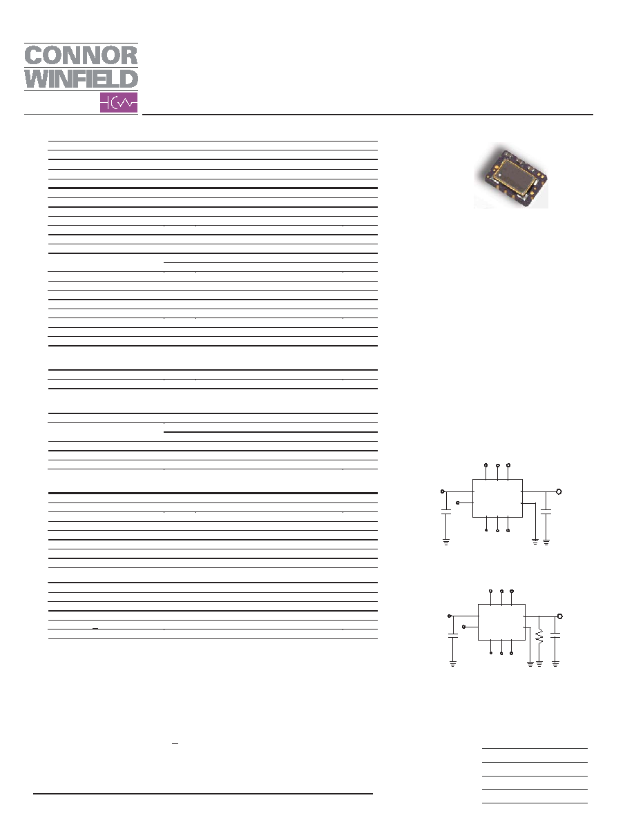
CMOS Test Circuit
Features
TA
5C
0713
20.0
Mhz
Clipped Sinewave Test Circuit
ABSOLUTE MAXIMUM RATINGS
TABLE 7.0
PARAMETER
UNITS
MINIMUM
NOMINAL
MAXIMUM
UNITS
NOTE
Storage Temperature
-55
-
125
°C
Supply Voltage
(Vcc)
-0.5
-
6.0
Vdc
Input Voltage
-0.5
-
Vcc+0.6
Vdc
Operating Specifications
Parameter
Minimum
Nominal
Maximum
UNITS
Notes
TCXO Frequency Calibration @ 25
°C
-1.00
-
1.00
ppm
1
Supply Voltage Variation. (Vcc±5%)
-0.2
-
0.2
ppm
Load Coefficient, ±5%
-0.2
-
0.2
ppm
Static Temperature Hysteresis
-0.4
-
0.4
ppm
2
Aging
-1.00
-
1.00
ppm / year
Frequency shift after reflow soldering
-1.00
-
1.00
ppm
Supply Voltage
(Vcc)
3.135
3.3
3.465
Vdc
3
(Vcc)
4.75
5.0
5.25
Vdc
3
Supply Current
(Icc)
-
6
10
mA
Jitter (BW=10Hz to 20MHz)
-
5
ps rms
Jitter (BW=12kHz to 20MHz)
-
1
ps rms
SSB Phase Noise at 10Hz offset
-
-80
-70
dBc/Hz
SSB Phase Noise at 100Hz offset
-
-110
-100
dBc/Hz
SSB Phase Noise at 1KHz offset
-
-135
-130
dBc/Hz
SSB Phase Noise at 10KHz offset
-
-150
-145
dBc/Hz
SSB Phase Noise at >100KHz offset
-
-150
dBc/Hz
Startup Time
-
10
ms
Input Characteristics for Enable / Disable Function (Pin 8)
Parameter
Minimum
Nominal
Maximum
Units
Notes
Enable Voltage (High) or open circuit
(Vih)
70% Vcc
-
Vdc
4
Disable Voltage (Low) Output Tri-stated
(Vil)
-
30% Vcc
Vdc
Input Characteristics for Voltage Control (Pin10)
Parameter
Minimum
Nominal
Maximum
Units
Notes
Control Voltage Range
(Vcc = 3.3V)
(Vc)
0.30
1.65
3.00
Vdc
(Vcc = 5.0V)
(Vc)
0.50
2.50
4.50
Vdc
Frequency Tuning measured @25
°C
±10
-
ppm
5
Linearity
±5
-
%
Slope
Positive
Input Impedance
100K
-
Ohms
CMOS Output Characteristics
Parameter
Minimum
Nominal
Maximum
Units
Notes
LOAD
-
15
-
pF
6
Voltage
(High)
(Voh)
90%Vcc
-
Vdc
(Low)
(Vol)
-
10%Vcc
Vdc
Current
(High)
(Ioh)
-
-4
mA
(Low)
(Iol)
4
-
mA
Duty Cycle at 50% of Vcc
455055
%
Rise / Fall Time 10% to 90%
-
8
ns
Clipped Sinewave Output Characteristics
Parameter
Minimum
Nominal
Maximum
Units
Notes
Load
7
Output Load Resistance
-
10K
-
Ohms
Output Load Capacitance
-
10
-
pF
Output Voltage (< 30 MHz)
1.00
-
V pk-pk
Output Voltage (> 30 MHz)
0.80
-
V pk-pk
3
5
4
8
7
6
2
1
10
9
Vcc
Supply
Voltage
DNC
DNC DNC
Output
15 pF**
.01 uF
Bypass
E/D
DNC = Do Not Connect
E/D = Enable / Disable
** NPO Grade component
Vcc
Supply
Voltage
.01 uF
Bypass
3
5
4
8
7
6
2
1
10
9
DNC
DNC DNC
Output
10 pF**
E/D
DNC = Do Not Connect
E/D = Enable / Disable
** NPO Grade component
10Kohm
1) TCXO: Initial calibration @ 25
°C. Specifications at time of shipment after 48
hours of operation.
2) Frequency change after reciprocal temperature ramped over the operating
range. Frequency measured before and after at 25°C.
3) For best in application performance, careful selection of an external power
source is critical. Select an external regulator that meets or exceeds to following
specifications regarding voltage regulation tolerance, initial accuracy,
temperature coefficient, voltage noise, and low voltage noise density.
Factory Test Conditions: Initial Accuracy ±2mv, Noise (0.1Hz to 10 KHz) 15uV
p-p, Voltage Noise Density = 50nV/sqrt Hz, Temperature Coefficient < 5ppm/°C.
4) Leave Pad 8 unconnected if enable / disable function is not required. When tri-
stated, the output stage is disabled but the oscillator and compensation circuit
are still active (current consumption < 1mA).
5) Additional pull ranges are available; please contact the factory for additional
information.
6) Attention: To achieve the frequency stability specified it is required that the
circuit connected to this TCXO output must have the equivalent input
capacitance that is specified by the nominal load capacitance.
7) Output is AC coupled.
.
相關(guān)PDF資料 |
PDF描述 |
|---|---|
| TC6E-010.24M | TCXO, CLOCK, 10.24 MHz, HCMOS OUTPUT |
| TA6F-010.24M | TCXO, CLOCK, 10.24 MHz, LVCMOS OUTPUT |
| TC6-ED7226/2 | 0.3 MHz - 490 MHz RF TRANSFORMER |
| TC7652CPAG | OP-AMP, 5000 uV OFFSET-MAX, 0.4 MHz BAND WIDTH, PDIP8 |
| TC7652CPDG | OP-AMP, 5000 uV OFFSET-MAX, 0.4 MHz BAND WIDTH, PDIP14 |
相關(guān)代理商/技術(shù)參數(shù) |
參數(shù)描述 |
|---|---|
| TA6C-020.0M | 制造商:CONNOR-WINFIELD 制造商全稱:Connor-Winfield Corporation 功能描述:High Precision TCXO / VCTCXO |
| TA6C12.000MTR | 制造商:TOKEN 制造商全稱:Token Electronics Industry Co., Ltd. 功能描述:CERAMIC CRYSTAL RESONATORS |
| TA6E-020.0M | 制造商:CONNOR-WINFIELD 制造商全稱:Connor-Winfield Corporation 功能描述:High Precision TCXO / VCTCXO |
| TA6F-020.0M | 制造商:CONNOR-WINFIELD 制造商全稱:Connor-Winfield Corporation 功能描述:High Precision TCXO / VCTCXO |
| TA6F10AHM3/6A | 功能描述:TVS 二極管 - 瞬態(tài)電壓抑制器 600watts 10V 5% Uni RoHS:否 制造商:Vishay Semiconductors 極性:Bidirectional 工作電壓: 擊穿電壓:58.9 V 鉗位電壓:77.4 V 峰值浪涌電流:38.8 A 系列: 封裝 / 箱體:DO-214AB 最小工作溫度:- 55 C 最大工作溫度:+ 150 C |
發(fā)布緊急采購(gòu),3分鐘左右您將得到回復(fù)。