- 您現(xiàn)在的位置:買賣IC網(wǎng) > PDF目錄383875 > T5504 (Lineage Power) Quad PCM Codecs with Filters(帶濾波器的四PCM編解碼器) PDF資料下載
參數(shù)資料
| 型號: | T5504 |
| 廠商: | Lineage Power |
| 元件分類: | Codec |
| 英文描述: | Quad PCM Codecs with Filters(帶濾波器的四PCM編解碼器) |
| 中文描述: | 四的PCM編解碼器和過濾器(帶濾波器的四的PCM編解碼器) |
| 文件頁數(shù): | 4/18頁 |
| 文件大小: | 334K |
| 代理商: | T5504 |
4
Lucent Technologies Inc.
Data Sheet
March 1999
T7504 and T5504 Quad PCM Codecs with Filters
Pin Information
(continued)
* I
d
Indicates a pull-down device is included on this lead.
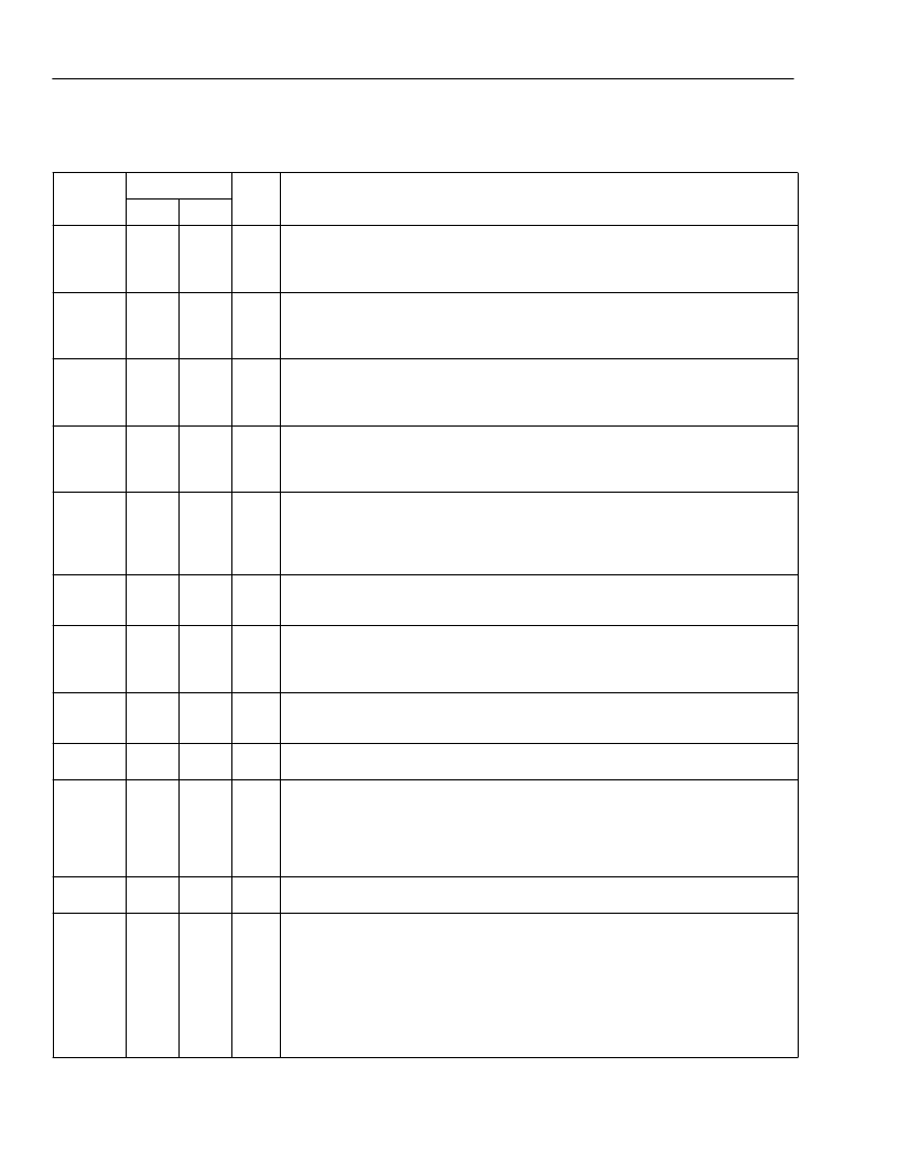
Table 1. Pin Descriptions
Symbol
Pin
Type
*
Name/Function
PLCC
14
8
16
22
13
9
17
21
12
10
18
20
7, 24
—
MQFP
15
8
19
26
14
9
20
25
13
10
21
24
3, 31
4, 30
VF
VF
VF
VF
GS
GS
GS
GS
VF
VF
VF
VF
V
DD
V
DDA
X
X
X
X
IN3
IN2
IN1
IN0
X
3
X
2
X
1
X
0
R
O3
R
O2
R
O1
R
O0
[1:0]
[1:0]
I
Voice Frequency Transmitter Input.
operational amplifier at the transmit filter input. Connect the signal to be digitized
to this pin through a resistor R
I
(see
Figure 2
).
Analog inverting input to the uncommitted
O
Gain Set for Transmitter.
amplifier. The pin is the input to the transmit differential filters. Connect the pin to
its corresponding VF
X
IN through a resistor R
Output of the transmit uncommitted operational
F
(see
Figure 2
).
O
Voice Frequency Receiver Output.
This pin can drive 2000
(or greater) loads.
—
5 V Digital and Analog Power Supplies
board. Each pin should be bypassed to ground with at least 0.1
as close to the device as possible. For the DIP and PLCC packages, V
both analog and digital internal circuits.
Analog Grounds
. All ground pins must be connected on the circuit board.
. All pins must be connected on the circuit
μ
F of capacitance
DD
serves
GNDA4
GNDA3
GNDA2
GNDA1
GNDA0
D
—
15
11
19
23
4
18
16
11
23
27
44
—
R
I
Receive PCM Data Input
ing edges of MCLK. Data is only entered for valid time slots as defined by the re-
lationship of the pulses on the FS
X
inputs and the pulse on the FSEP input.
Transmit PCM Data Output
. This pin remains in the high-impedance state except
during active transmit time slots. An active transmit time slot is defined as one in
which a pulse is present on one of the FSx inputs. Data is shifted out on the rising
edge of MCLK.
Master Clock Input
. The frequency must be 2.048 MHz or 4.096 MHz. This clock
serves as the bit clock for all PCM data transfer. A 40% to 60% duty cycle is re-
quired.
Digital Ground
. Ground connection for the digital circuitry. All ground pins must be
connected on the circuit board.
Transmit Frame Sync
. This signal is an edge trigger and must be high for a min-
imum of one MCLK cycle. This signal must be derived from MCLK. The division ra-
tio is 1:256 or 1:512 (FS
X
:MCLK). Each FS
start of the desired active output time slot. Pulses on the various FS
be separated by one or more integer multiples of time slots. An internal pull-down
device is included on each FS
X
.
A-Law/
μ
-Law Select
. A logic low selects
coding. A pull-down device is included.
Frame Sync Separation
. The pulse width of this 8 kHz signal defines the timing
offset between the transmit and receive frames. Internally generated receive frame
sync pulses are delayed from the corresponding transmit frame sync pulse rising
edge by one less than the FSEP pulse width in negative MCLK edges. If the pulse
width is one MCLK period or less, the transmit and receive frame syncs are made
coincident. Loss of FSEP causes the device to powerdown. If the master clock fre-
quency is 2.048 MHz or 4.096 MHz, delays of 255 or 511 clock pulses are not al-
lowed, respectively. Timing relationships between FSEP, FS
given in Figures
6
—
9
.
. The data on this pin is shifted into the device on the fall-
D
X
3
43
O
MCLK
5
1
I
GNDD
2
41
—
FS
FS
FS
FS
X
X
X
X
3
2
1
0
28
27
26
25
36
35
34
33
I
d
X
input must have a pulse present at the
X
inputs must
ASEL
6
2
I
d
μ
-law coding. A logic high selects A-law
FSEP
1
37
I
X
N, and time slot 0 are
相關(guān)PDF資料 |
PDF描述 |
|---|---|
| T70HF10 | POWER RECTIFIER DIODES |
| T70HF100 | POWER RECTIFIER DIODES |
| T70HF120 | POWER RECTIFIER DIODES |
| T70HF | CONTACTOR? COIL 120VAC NEMA |
| T70HF20 | POWER RECTIFIER DIODES |
相關(guān)代理商/技術(shù)參數(shù) |
參數(shù)描述 |
|---|---|
| T-55040GD020JU-LW-AGN | 功能描述:TFT 顯示器 & 附件 2.0" 240x320 Transmissive RoHS:否 制造商:Sharp Microelectronics 產(chǎn)品:Displays 對角線:1.35 in 分辨率:96 x 96 模塊大小 - 寬x高x厚:28.2 mm x 32.34 mm x 1.4 mm 觀察區(qū)域 - 寬x高:24.192 mm x 24.192 mm 附加的觸摸屏:No 接口:Serial 背光: 背景色: 電源電壓:3 V 工作電流: 工作溫度范圍:- 10 C to + 60 C 封裝: |
| T55-04M | 制造商:The Cherry Corporation 功能描述: |
| T55-04MC | 制造商:The Cherry Corporation 功能描述: |
| T5504ML | 制造商:Alcatel-Lucent 功能描述:PCM CODEC, Quad, 28 Pin, Plastic, PLCC |
| T-5504-ML-D | 制造商:Alcatel-Lucent 功能描述: |
發(fā)布緊急采購,3分鐘左右您將得到回復(fù)。