- 您現(xiàn)在的位置:買賣IC網(wǎng) > PDF目錄385894 > SY89423V (Micrel Semiconductor,Inc.) 5V/3.3V DUAL HIGH-PERFORMANCE PHASE LOCKED LOOP PDF資料下載
參數(shù)資料
| 型號(hào): | SY89423V |
| 廠商: | Micrel Semiconductor,Inc. |
| 英文描述: | 5V/3.3V DUAL HIGH-PERFORMANCE PHASE LOCKED LOOP |
| 中文描述: | 5V/3.3V雙高性能鎖相環(huán) |
| 文件頁數(shù): | 3/8頁 |
| 文件大小: | 98K |
| 代理商: | SY89423V |
3
ClockWorks
SY89423V
Micrel
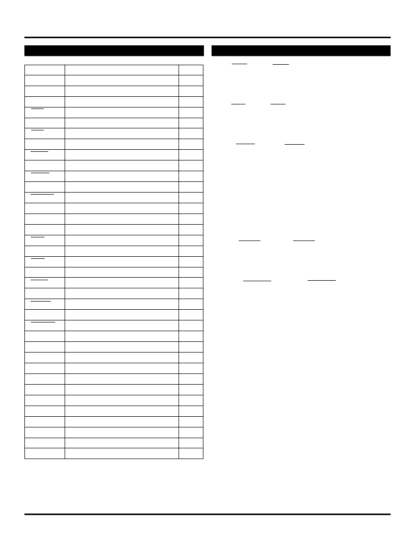
Pin
Function
I/O
I/O
F1A
Filter Pin 1A
F2A
Filter Pin 2A
I/O
RINA
Inverted Reference Input A
I
RINA
Reference Input A
I
FINA
Feedback Input A
I
FINA
Inverted Feedback Input A
I
HFINA
High Frequency Input A
I
HFINA
Inverted High Frequency Input A
I
FOUTA
Frequency Output A
O
FOUTA
Inverted Frequency Output A
O
HFOUTA
High Frequency Output A
O
HFOUTA
Inverted High Frequency Output A
O
F1B
Filter Pin 1B
I/O
F2B
Filter Pin 2B
I/O
RINB
Reference Input B
I
RINB
Inverted Reference Input B
I
FINB
Feedback Input B
I
FINB
Inverted Feedback Input B
I
HFINB
High Frequency Input B
I
HFINB
Inverted High Frequency Input B
I
FOUTB
Frequency Output B
O
FOUTB
Inverted Frequency Output B
O
HFOUTB
High Frequency Output B
O
HFOUTB
Inverted Frequency Output B
O
V
CC
V
CC
—
V
CCOA
Output V
CC
—
V
CCOB
Output V
CC
—
V
EE
V
EE
(0V)
—
S1A
Select Input 1A (TTL)
I
S2A
Select Input 2A (TTL)
I
S3A
Select Input 3A (TTL)
I
S1B
Select Input 1B (TTL)
I
S2B
Select Input 2B (TTL)
I
S3B
Select Input 3B (TTL)
I
S4B
Select Input 4B (TTL)
I
S5B
Select Input 5B (TTL)
I
RINA, RINA, RINB, RINB
Reference frequency inputs for loop A and B. These are
differential signal pairs and may be driven differentially or
single-ended.
FINA, FINA, FINB, FINB
Feedback frequency inputs for loop A and B. These are
differential signal pairs and may be driven differentially or
single-ended.
HFINA, HFINA, HFINB, HFINB
High frequency feedback inputs. Differential drive is
recommended.
F1A, F2A, F1B, F2B
These pins are connection points for the loop filters, which are
to be provided off-chip. F1X is the high impedance side, F2X
is the reference side. The loop filter should be a first order, low
pass with a DC block. The difference voltage on these pins will
be a DC level, which is controlled by the loop feedback and
determined by the required VCO frequency.
FOUTA, FOUTA, FOUTB, FOUTB
Frequency outputs for the loops. These are differential, positive
referenced, emitter-follower signals and must be terminated
off-chip. Termination in 50 ohms is recommended.
HFOUTA, HFOUTA, HFOUTB, HFOUTB
High frequency outputs. These are differential, positive
referenced, emitter-follower signals and must be terminated
off-chip. Termination in 50 ohms is recommended.
S1A, S2A, S3A, S1B, S2B, S3B, S4B, S5B
These inputs are used to select the configuration for PLLA and
PLLB. See the Frequency Selection Table for details of the
logic.
V
CC
This is the positive supply for the chip. It should be decoupled
and present a low impedance in order to assure low-jitter
operation.
V
CCOA
, V
CCOB
These are the positive supplies for the output buffers. They are
constrained to be equal to or less than the value of V
CC
.
V
EE
This pin is the negative supply for the chip and is normally
connected to ground (0V).
PIN NAMES
PIN DESCRIPTION
相關(guān)PDF資料 |
PDF描述 |
|---|---|
| SY89423VJCTR | 5V/3.3V DUAL HIGH-PERFORMANCE PHASE LOCKED LOOP |
| SY89424VZCTR | 5V/3.3V FREQUENCY SYNTHESIZER 60MHz to 1GHz |
| SY89424V | 5V/3.3V FREQUENCY SYNTHESIZER 60MHz to 1GHz |
| SY89425JC | DUAL SONET OC-12 CLOCK SYNTHESIZER |
| SY89425 | Dual Sonet OC-12 Clock Synthesizer(雙鎖相環(huán)時(shí)鐘合成器(由兩個(gè)Sonet兼容時(shí)鐘發(fā)生器組成)) |
相關(guān)代理商/技術(shù)參數(shù) |
參數(shù)描述 |
|---|---|
| SY89423V_07 | 制造商:MICREL 制造商全稱:Micrel Semiconductor 功能描述:5V/3.3V DUAL HIGH-PERFORMANCE |
| SY89423VJC | 制造商:MICREL 制造商全稱:Micrel Semiconductor 功能描述:5V/3.3V DUAL HIGH-PERFORMANCE PHASE LOCKED LOOP |
| SY89423VJCTR | 制造商:MICREL 制造商全稱:Micrel Semiconductor 功能描述:5V/3.3V DUAL HIGH-PERFORMANCE |
| SY89424V | 制造商:MICREL 制造商全稱:Micrel Semiconductor 功能描述:5V/3.3V FREQUENCY SYNTHESIZER 60MHz to 1GHz |
| SY89424VZC | 制造商:Micrel Inc 功能描述:IC, PHASE LOCK LOOP, 1GHZ, W16-SOIC, PLL Type:Frequency Synthesis, Frequency:1GH |
發(fā)布緊急采購,3分鐘左右您將得到回復(fù)。