- 您現(xiàn)在的位置:買賣IC網(wǎng) > PDF目錄372297 > ST25C02B3 IC FLEX 10KE FPGA 50K 240-PQFP PDF資料下載
參數(shù)資料
| 型號(hào): | ST25C02B3 |
| 英文描述: | IC FLEX 10KE FPGA 50K 240-PQFP |
| 中文描述: | I2C串行EEPROM的 |
| 文件頁(yè)數(shù): | 9/16頁(yè) |
| 文件大小: | 145K |
| 代理商: | ST25C02B3 |
第1頁(yè)第2頁(yè)第3頁(yè)第4頁(yè)第5頁(yè)第6頁(yè)第7頁(yè)第8頁(yè)當(dāng)前第9頁(yè)第10頁(yè)第11頁(yè)第12頁(yè)第13頁(yè)第14頁(yè)第15頁(yè)第16頁(yè)
Multibyte Write.
For the Multibyte Write mode, the
MODE pin must be at V
IH
. The Multibyte Write
mode can be started from any address in the
memory. The master sends from one up to 4 bytes
of data, which are each acknowledged by the mem-
ory. The transfer is terminated by the master gen-
erating a STOP condition. The duration of the write
cycle is t
W
= 10ms maximum except when bytes
are accessed on 2 rows (that is have different
values for the 6 most significant address bits A7-
A2), the programming time is then doubled to a
maximum of 20ms. Writing more than 4 bytes in the
Multibyte Write mode may modify data bytes in an
adjacent row (one row is 8 bytes long). However,
the Multibyte Write can properly write up to 8
consecutive bytes only if the first address of these
8 bytes is the first address of the row, the 7 following
bytes being written in the 7 following bytes of this
same row.
Page Write.
For the Page Write mode, the MODE
pin must be at V
IL
. The Page Write mode allows up
to 8 bytes to be written in a single write cycle,
provided that they are all located in the same ’row’
in the memory: that is the 5 most significant mem-
ory address bits (A7-A3) are the same. The master
sends from one up to 8 bytes of data, which are
each acknowledged by the memory. After each
byte is transfered, the internal byte address counter
(3 least significant bits only) is incremented. The
transfer is terminated by the master generating a
STOP condition. Care must be taken to avoid ad-
dress counter ’roll-over’ which could result in data
being overwritten. Note that, for any write mode,
the generation by the master of the STOP condition
starts the internal memory program cycle. All inputs
are disabled until the completion of this cycle and
the memory will not respond to any request.
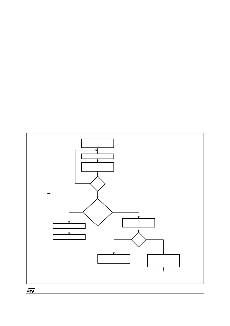
WRITE Cycle
in Progress
AI01099B
Next
Operation is
Addressing the
Memory
START Condition
DEVICE SELECT
with RW = 0
ACK
Returned
YES
NO
YES
NO
ReSTART
STOP
Proceed
WRITE Operation
Proceed
Random Address
READ Operation
Send
Byte Address
First byte of instruction
with RW = 0 already
decoded by ST24xxx
Figure 7. Write Cycle Polling using ACK
9/16
ST24/25C02, ST24C02R, ST24/25W02
相關(guān)PDF資料 |
PDF描述 |
|---|---|
| ST25C02B6 | IC FLEX 10KE FPGA 50K 240-PQFP |
| ST25C02M1 | MAX II CPLD 1270 LE 144-TQFP |
| ST25C02M3 | Stratix II FPGA 60K FBGA-484 |
| ST25C02M6 | Cyclone II FPGA 70K FBGA-672 |
| ST25W02B6 | Cyclone FPGA 12K FBGA-256 |
相關(guān)代理商/技術(shù)參數(shù) |
參數(shù)描述 |
|---|---|
| ST25C02B3TR | 制造商:STMICROELECTRONICS 制造商全稱:STMicroelectronics 功能描述:SERIAL 2K (256 x 8) EEPROM |
| ST25C02B5TR | 制造商:STMICROELECTRONICS 制造商全稱:STMicroelectronics 功能描述:SERIAL 2K (256 x 8) EEPROM |
| ST25C02B6 | 制造商:未知廠家 制造商全稱:未知廠家 功能描述:I2C Serial EEPROM |
| ST25C02B6TR | 制造商:STMICROELECTRONICS 制造商全稱:STMicroelectronics 功能描述:SERIAL 2K (256 x 8) EEPROM |
| ST25C02M1 | 制造商:未知廠家 制造商全稱:未知廠家 功能描述:I2C Serial EEPROM |
發(fā)布緊急采購(gòu),3分鐘左右您將得到回復(fù)。