- 您現(xiàn)在的位置:買賣IC網(wǎng) > PDF目錄1969 > SP505BCM-L (Exar Corporation)IC TXRX WAN MULTI-MODE 80LQFP PDF資料下載
參數(shù)資料
| 型號: | SP505BCM-L |
| 廠商: | Exar Corporation |
| 文件頁數(shù): | 11/35頁 |
| 文件大小: | 0K |
| 描述: | IC TXRX WAN MULTI-MODE 80LQFP |
| 標(biāo)準(zhǔn)包裝: | 84 |
| 類型: | 收發(fā)器 |
| 驅(qū)動器/接收器數(shù): | 7/7 |
| 規(guī)程: | 多協(xié)議 |
| 電源電壓: | 5V |
| 安裝類型: | 表面貼裝 |
| 封裝/外殼: | 80-LQFP |
| 供應(yīng)商設(shè)備封裝: | 80-LQFP(14x14) |
| 包裝: | 托盤 |
第1頁第2頁第3頁第4頁第5頁第6頁第7頁第8頁第9頁第10頁當(dāng)前第11頁第12頁第13頁第14頁第15頁第16頁第17頁第18頁第19頁第20頁第21頁第22頁第23頁第24頁第25頁第26頁第27頁第28頁第29頁第30頁第31頁第32頁第33頁第34頁第35頁
9
Exar Coporation 48720 Kato Road, Fremont CA, 94538 (50) 668-7000 Fax (50) 668-707 www.exar.com
SP505_00_08308
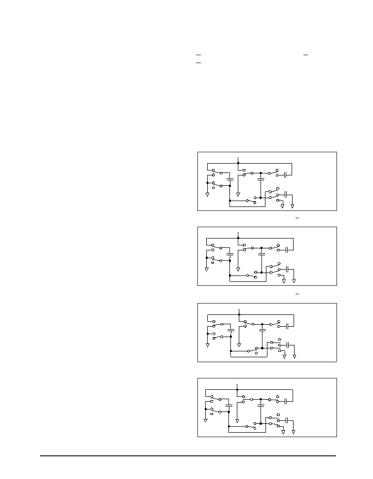
Phase 2 (±10V)
— V
SS transfer — Phase two of the clock
connects the negative terminal of C
2 to
the V
SS storage capacitor and the positive
terminal of C
2 to ground, and transfers the
generated –l0V or the generated –5V to C
3.
Simultaneously,thepositivesideofcapacitor
C
is switched to +5V and the negative side
is connected to ground.
Phase 2 (±5V)
— V
SS & VDD charge storage — C
+
is recon-
nected to V
CC to recharge the C capacitor.
C
2
+
isswitchedtogroundandC
2
–
isconnected
to C
3. The 5V charge from Phase is now
transferred to the V
SS storage capacitor. VSS
receives a continuous charge from either C
or C
2. With the C capacitor charged to 5V,
the cycle begins again.
Phase 3
— V
DD charge storage — The third phase
of the clock is identical to the first phase
— the charge transferred in C
produces
–5V in the negative terminal of C
, which
is applied to the negative side of capacitor
C
2. Since C2
+
is at +5V, the voltage potential
across C
2 is l0V. For the 5V output, C2
+
is
connected to ground so that the potential
on C
2 is only +5V.
Phase 4
— V
DD transfer — The fourth phase of the
clock connects the negative terminal of C
2
to ground and transfers the generated l0V
or the generated 5V across C
2 to C4, the VDD
storage capacitor. Again, simultaneously
with this, the positive side of capacitor C
is switched to +5V and the negative side is
connected to ground, and the cycle begins
again.
Since both V
DD and VSS are separately gen-
erated from V
CC in a no–load condition, VDD
and V
SS will be symmetrical. Older charge
pump approaches that generate V– from
V+ will show a decrease in the magnitude
of V– compared to V+ due to the inherent
inefficiencies in the design.
The clock rate for the charge pump typically
operates at 5kHz. The external capacitors
must be a minimum of 22F with a 6V
breakdown rating.
External Power Supplies
For applications that do not require +5V
only, external supplies can be applied at the
V+ and V– pins. The value of the external
supply voltages must be no greater than
+l0.5V. The tolerance should be +5% from
+0V. The current drain for the supplies is
used for RS-232 and RS-423 drivers. For
the RS-232 driver, the current requirement
will be 3.5mA per driver. The RS-423 driver
worst case current drain will be mA per
driver. Power sequencing is required for the
SP505. The supplies must be sequenced
accordingly: +0V, +5V and –0V. It is
important to prevent V
SS from starting up
before V
CC or VDD.
Figure 47. Charge Pump Phase 2 for +0V.
Figure 49. Charge Pump Phase 3.
V CC = +5V
–1 0V
V DD S torage C apa citor
C 1
C 2
C 4
+
–
VSS Storage C apa citor
C 3
+
–
V CC = +5V
–5 V
+5V
V DD S torage C apa citor
C 1
C 2
C 4
+
–
VSS S torage C apa citor
C 3
+
–
Figure 50. Charge Pump Phase 4.
Figure 48. Charge Pump Phase 2 for +5V.
V CC = +5V
V DD S torage C apa citor
C 1
C 2
C 4
+
–
VSS S torage C apa citor
C 3
+
–
–5 V
V CC = +5V
+10V
V DD S torage C apa citor
C 1
C 2
C 4
+
–
VSS S torage C apa citor
C 3
+
–
相關(guān)PDF資料 |
PDF描述 |
|---|---|
| SP506CM-L | IC TXRX WAN MULTI-MODE 80LQFP |
| SP507CM-L | IC TXRX WAN MULTI-MODE 80LQFP |
| SP508EF-L | IC TXRX MULTIPROTOCOL 100LQFP |
| SP510CM-L | IC TXRX MULTIPROTOCOL HS 100LQFP |
| SP526CF-L | IC TXRX WAN MULTI-MODE 44LQFP |
相關(guān)代理商/技術(shù)參數(shù) |
參數(shù)描述 |
|---|---|
| SP505CF | 制造商:SIPEX 制造商全稱:Sipex Corporation 功能描述:Multi-Protocol Serial Transceivers |
| SP505EB | 制造商:SIPEX 制造商全稱:Sipex Corporation 功能描述:Multi-Protocol Serial Transceivers |
| SP505EK | 制造商:SIPEX 制造商全稱:Sipex Corporation 功能描述:Multi-Protocol Serial Transceivers |
| SP505P | 制造商:SII 制造商全稱:Seiko Instruments Inc 功能描述:LIQUID CRYSTAL DISPLAYS(STANDARD PRODUCTS) |
| SP505RB | 制造商:SIPEX 制造商全稱:Sipex Corporation 功能描述:Multi-Protocol Serial Transceivers |
發(fā)布緊急采購,3分鐘左右您將得到回復(fù)。