- 您現(xiàn)在的位置:買賣IC網(wǎng) > PDF目錄299918 > SP319CM-L 7 LINE TRANSCEIVER, PQFP80 PDF資料下載
參數(shù)資料
| 型號: | SP319CM-L |
| 元件分類: | Buffer和線驅(qū)動 |
| 英文描述: | 7 LINE TRANSCEIVER, PQFP80 |
| 封裝: | MS-026BEC, LQFP-80 |
| 文件頁數(shù): | 8/15頁 |
| 文件大小: | 143K |
| 代理商: | SP319CM-L |
2
Rev. 6/10/03
SP319 10Mbps, +5V-Only V.35 Interface with RS-232 (V.28) Control Lines
Copyright 2003 Sipex Corporation
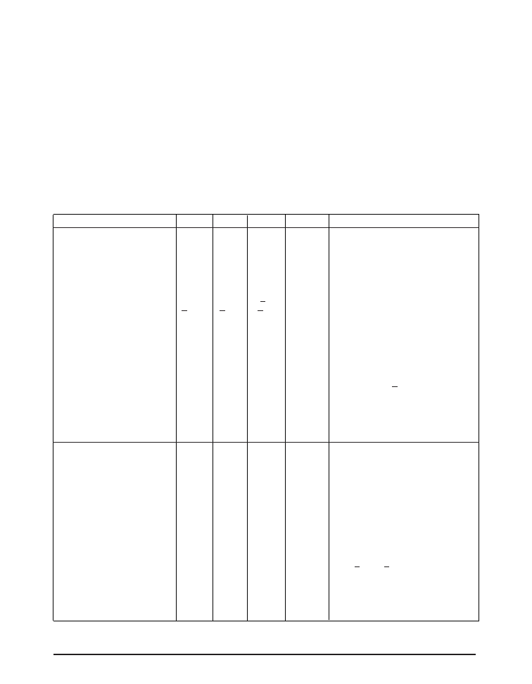
ABSOLUTE MAXIMUM RATINGS
These are stress ratings only and functional operation of the device at
these ratings or any other above those indicated in the operation
sections of the specifications below is not implied. Exposure to absolute
maximum rating conditions for extended periods of time may affect
reliability.
V
CC.....................................................................................................+7V
Input Voltages
Logic........................................................-0.3V to (V
CC+0.5V)
Drivers..................................................-0.3V to (V
CC+0.5V)
Receivers..................................................±30V at ≤100mA
Output Voltages
Logic........................................................-0.3V to (V
CC+0.5V)
Drivers.......................................................................±14V
Receivers..............................................-0.3V to (V
CC+0.5V)
Storage Temperature.......................................................-65C to +150C
Power Dissipation per Package
80-pin QFP (derate 18.3mW/oC above +70oC)..........................1500mW
ELECTRICAL SPECIFICATIONS
T
AMB = TMIN to TMAX and VCC = 5V±5% unless otherwise noted.
PARAMETER
MIN.
TYP.
MAX.
UNITS
CONDITIONS
V.35 DRIVER
TTL Input Levels
V
IL
0.8
Volts
V
IH
2.0
Volts
Voltage Outputs
Open Circuit Voltage
+1.2
Volts
Refer to
Figure 1
Differential Outputs
+0.44
+0.55
+0.66
Volts
R
L=100 from A to B; Figure 2
Source Impedance
50
100
150
Ohms
Figure 4
Short Circuit Impedance
135
150
165
Ohms
Measured from A=B to Gnd,
V
OUT=-2V to +2V; Figure 5; TAMB = +25
oC
Voltage Output Offset
-0.6
+0.6
Volts
V
Offset={[|VA|+|VB|]/2}; Figure 3
AC Characteristics
T
AMB = +25
oC for all AC parameters
Transition Time
40
ns
10% to 90%;
Figure 6
Maximum Transmission Rate
10
Mbps
V
DIFF OUT= 0.55V+20% ; Figure 9
Propagation Delay
t
PHL
80
100
ns
Measured from 1.5V of V
IN
to 50% of V
OUT; Figure 9, 10
t
PLH
80
100
ns
Measured from 1.5V of V
IN
to 50% of V
OUT; Figure 9, 10
V.35 RECEIVER
TTL Output Levels
V
OL
0.4
Volts
I
OUT=-3.2mA
V
OH
2.4
Volts
I
OUT=1.0mA
Receiver Inputs
Differential Input
Threshold
-0.3
+0.3
Volts
Input Impedance
90
100
110
Ohms
Figure 7
Short Circuit Impedance
135
150
165
Ohms
Measured from A=B to Gnd
V
IN=-2V to +2V; Figure 8; TAMB = +25
oC
AC Characteristics
T
AMB = +25
oC for all AC parameters
Maximum Transmission Rate
10
Mbps
V
IN = +0.55V +20%; Figure 9
Propagation Delay
t
PHL
60
80
ns
Measured from 50% of V
IN to
1.5V of R
OUT; Figure 9, 11
t
PLH
60
80
ns
Measured from 50% of V
IN to
1.5V of R
OUT; Figure 9, 11
相關(guān)PDF資料 |
PDF描述 |
|---|---|
| SP5769/KG/MP1T | PLL FREQUENCY SYNTHESIZER, 3000 MHz, PDSO16 |
| SP6659EK1-1.5/TR | 1.3 A SWITCHING REGULATOR, 1800 kHz SWITCHING FREQ-MAX, PDSO5 |
| SP7800ABN | 1-CH 12-BIT SUCCESSIVE APPROXIMATION ADC, PARALLEL ACCESS, PDIP24 |
| SP7800AAS | 1-CH 12-BIT SUCCESSIVE APPROXIMATION ADC, PARALLEL ACCESS, PDSO24 |
| SP7800ABS | 1-CH 12-BIT SUCCESSIVE APPROXIMATION ADC, PARALLEL ACCESS, PDSO24 |
相關(guān)代理商/技術(shù)參數(shù) |
參數(shù)描述 |
|---|---|
| SP31R0JT | 功能描述:電流傳感電阻器 - SMD SP3 1R0 5% TAPED RoHS:否 制造商:Vishay/Dale 電阻:10 mOhms 功率額定值:1 W 容差:1 % 外殼代碼 - in:2512 外殼代碼 - mm:6432 溫度系數(shù):75 PPM / C 系列:WSL 工作溫度范圍:- 65 C to + 170 C 產(chǎn)品:Power Metal Strip Resistors Low Value |
| SP32 | 制造商:VOLT PLASTICS 功能描述: |
| SP-32 | 制造商:Triad Magnetics 功能描述: |
| SP3-2.5-10 | 制造商:RHOMBUS-IND 制造商全稱:Rhombus Industries Inc. 功能描述:SP3 Series Mini-SIP Passive Delay Modules |
| SP3-2.5-20 | 制造商:RHOMBUS-IND 制造商全稱:Rhombus Industries Inc. 功能描述:SP3 Series Mini-SIP Passive Delay Modules |
發(fā)布緊急采購,3分鐘左右您將得到回復(fù)。