- 您現(xiàn)在的位置:買賣IC網(wǎng) > PDF目錄372167 > SP1490EEP Full Duplex RS-485 Transceivers PDF資料下載
參數(shù)資料
| 型號(hào): | SP1490EEP |
| 元件分類: | RS-485 |
| 英文描述: | Full Duplex RS-485 Transceivers |
| 中文描述: | 全雙工RS - 485接口收發(fā)器 |
| 文件頁數(shù): | 2/10頁 |
| 文件大小: | 73K |
| 代理商: | SP1490EEP |
2
Date: 5/18/04
SP1490E/1491E Full Duplex RS-485 Transceivers
Copyright 2004 Sipex Corporation
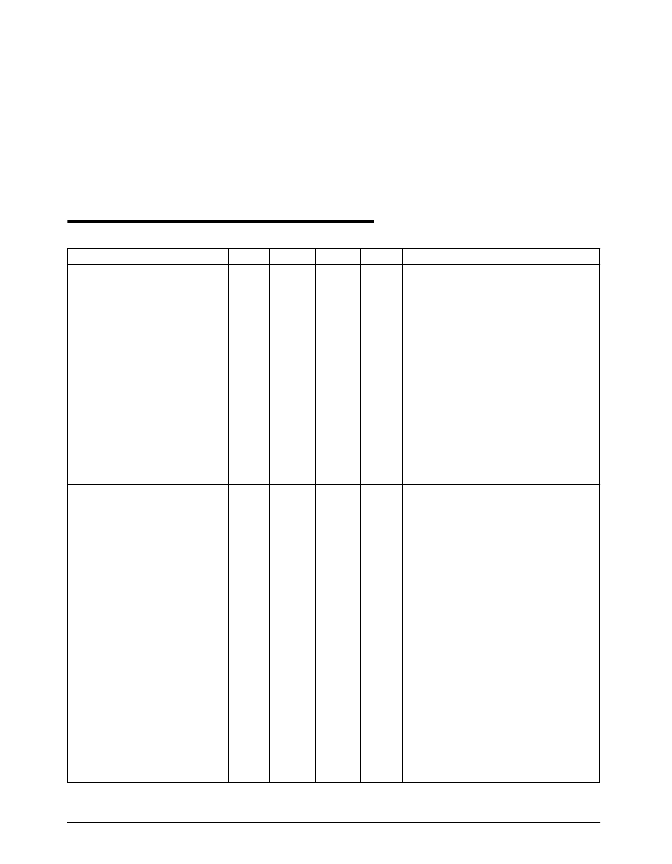
ABSOLUTE MAXIMUM RATINGS
These are stress ratings only and functional operation of the device at
these ratings or any other above those indicated in the operation sections
of the specifications below is not implied. Exposure to absolute maximum
rating conditions for extended periods of time may affect reliability.
V
...................................................................................................+7V
Input Voltages
Drivers................................................-0.5V to (V
+0.5V)
Receivers..................................................................
±
14V
Output Voltages
Drivers......................................................................
14V
Receivers...........................................-0.5V to (V
+0.5V)
Storage Temperature....................................................-65
C to +150
Power Dissipation.....................................................................1000mW
T
MIN
to T
MAX
and V
CC
= 5V
±
5% unless otherwise noted.
PARAMETERS
SP1490E/1491E DRIVER
DC Characteristics
Differential Output Voltage
Differential Output Voltage
MIN.
TYP.
MAX.
UNITS
CONDITIONS
3.5
2
V
CC
V
CC
Volts
Volts
Unloaded; R =
∞
;
see figure 1
With Load; R = 50
; (RS422);
see figure 1
With Load; R = 27
; (RS485);
see figure 1
Differential Output Voltage
Change in Magnitude of Driver
Differential Output Voltage for
Complimentary States
Driver Common-Mode
Output Voltage
Input High Voltage
Input Low Voltage
Input Current
Driver Short-Circuit Current
V
OUT
= HIGH
V
OUT
= LOW
1.5
V
CC
Volts
0.2
Volts
R = 27
or R = 50
;
see figure 1
3
Volts
Volts
Volts
μ
A
R = 27
or R = 50
;
see figure 1
Applies to D
Applies to D
Applies to D
2.0
0.8
±
10
±
250
±
250
mA
mA
-7V
≤
V
O
≤
+12V
-7V
≤
V
O
≤
+12V
SP1490E/1491E DRIVER
AC Characteristics
Maximum Data Rate
Driver Input to Output
20
Mbps
ns
30
40
t
; R
= 54
, C
L1
= C
L2
= 100pF;
see figures 3 and 6
t
; R
= 54
, C
L1
= C
L2
= 100pF;
see figures 3 and 6
see figures 3 and 6,
t
= | t
- t
|
From 10% to 90%; R
DIFF
= 54
,
Driver Input to Output
30
40
ns
Driver Skew
5
ns
Driver Rise or Fall Time 8
20
ns
SP1491E only
C
L1
= C
L2
= 100pF;
see figures 3 and 6
t
R/F
C
= C
L2
= 100pF;
see figures
4 and 7;
S
closed
C
= C
L2
= 100pF;
see figures
4 and 7;
S
closed
C
= C
L2
= 100pF;
see figures
4 and 7;
S
closed
C
= C
L2
= 100pF;
see figures
4 and 7;
S
2
closed
Driver Enable to Output High
20
70
ns
Driver Enable to Output Low
40
70
ns
Driver Disable Time from Low
40
70
ns
Driver Disable Time from High
40
70
ns
ELECTRICAL CHARACTERISTICS
相關(guān)PDF資料 |
PDF描述 |
|---|---|
| SP1491E | Full Duplex RS-485 Transceivers |
| SP1491ECN | Full Duplex RS-485 Transceivers |
| SP1491ECP | Full Duplex RS-485 Transceivers |
| SP1491EEN | Full Duplex RS-485 Transceivers |
| SP1491EEP | Full Duplex RS-485 Transceivers |
相關(guān)代理商/技術(shù)參數(shù) |
參數(shù)描述 |
|---|---|
| SP1490EEP-L | 制造商:Exar Corporation 功能描述: |
| SP1490ETR | 制造商:SIPEX 制造商全稱:Sipex Corporation 功能描述:Full Duplex RS-485 Transceivers |
| SP1491E | 制造商:SIPEX 制造商全稱:Sipex Corporation 功能描述:Full Duplex RS-485 Transceivers |
| SP1491ECN | 制造商:SIPEX 制造商全稱:Sipex Corporation 功能描述:Full Duplex RS-485 Transceivers |
| SP1491ECN/TR | 制造商:SIPEX 制造商全稱:Sipex Corporation 功能描述:Full Duplex RS-485 Transceivers |
發(fā)布緊急采購,3分鐘左右您將得到回復(fù)。