- 您現(xiàn)在的位置:買賣IC網(wǎng) > PDF目錄98123 > SN74LVC1GU04YEAR (TEXAS INSTRUMENTS INC) LVC/LCX/Z SERIES, 1-INPUT INVERT GATE, PBGA5 PDF資料下載
參數(shù)資料
| 型號: | SN74LVC1GU04YEAR |
| 廠商: | TEXAS INSTRUMENTS INC |
| 元件分類: | 門電路 |
| 英文描述: | LVC/LCX/Z SERIES, 1-INPUT INVERT GATE, PBGA5 |
| 封裝: | MO-211EA, DSBGA-5 |
| 文件頁數(shù): | 11/17頁 |
| 文件大小: | 610K |
| 代理商: | SN74LVC1GU04YEAR |
www.ti.com
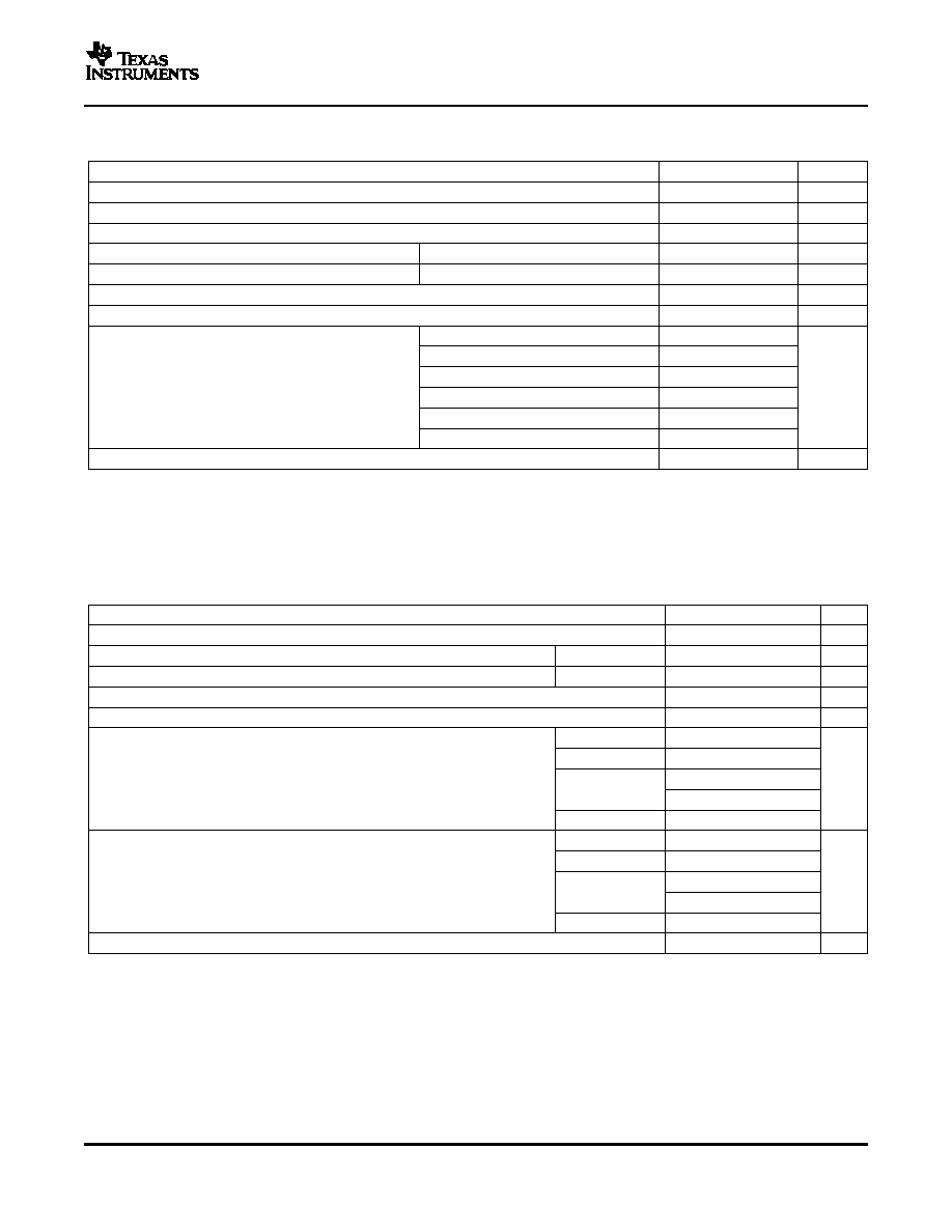
Absolute Maximum Ratings
(1)
Recommended Operating Conditions
(1)
SINGLE INVERTER GATE
SCES215S – APRIL 1999 – REVISED OCTOBER 2006
over operating free-air temperature range (unless otherwise noted)
RATING
UNIT
VCC
Supply voltage range
–0.5 to 6.5
V
VI
Input voltage range (2)
0.5 to 6.5
V
VO
Voltage range applied to any output in the high or low state (2)(3)
–0.5 to VCC + 0.5
V
IIK
Input clamp current
VI < 0
–50
mA
IOK
Output clamp current
VO < 0
–50
mA
IO
Continuous output current
±50
mA
Continuous current through VCC or GND
±100
mA
DBV package
206
DCK package
252
DRL package
142
θ
JA
Package thermal impedance(4)
°C/W
YEA/YZA package
154
YEP/YZP package
132
YZV package
116
Tstg
Storage temperature range
–65 to 150
°C
(1)
Stresses beyond those listed under "absolute maximum ratings" may cause permanent damage to the device. These are stress ratings
only, and functional operation of the device at these or any other conditions beyond those indicated under "recommended operating
conditions" is not implied. Exposure to absolute-maximum-rated conditions for extended periods may affect device reliability.
(2)
The input and output negative-voltage ratings may be exceeded if the input and output current ratings are observed.
(3)
The value of VCC is provided in the recommended operating conditions table.
(4)
The package thermal impedance is calculated in accordance with JESD 51-7.
MIN
MAX
UNIT
VCC
Supply voltage
1.65
5.5
V
VIH
High-level input voltage
IO = –100 A
0.75
× V
CC
V
VIL
Low-level input voltage
IO = 100 A
0.25
× V
CC
V
VI
Input voltage
0
5.5
V
VO
Output voltage
0
VCC
V
VCC = 1.65 V
–4
VCC = 2.3 V
–8
IOH
High-level output current
–16
mA
VCC = 3 V
–24
VCC = 4.5 V
–32
VCC = 1.65 V
4
VCC = 2.3 V
8
IOL
Low-level output current
16
mA
VCC = 3 V
24
VCC = 4.5 V
32
TA
Operating free-air temperature
–40
85
°C
(1)
All unused inputs of the device must be held at VCC or GND to ensure proper device operation. Refer to the TI application report,
Implications of Slow or Floating CMOS Inputs, literature number SCBA004.
3
相關PDF資料 |
PDF描述 |
|---|---|
| SN74LVC1GX04YZPR | LVC/LCX/Z SERIES, 1-INPUT INV/NINV GATE, BGA6 |
| SN74LVC1T45DCKRG4 | LVC/LCX/Z SERIES, 1-BIT TRANSCEIVER, TRUE OUTPUT, PDSO6 |
| SN74LVC2244ADGVRG4 | LVC/LCX/Z SERIES, DUAL 4-BIT DRIVER, TRUE OUTPUT, PDSO20 |
| SN74LVC2244APWE4 | LVC/LCX/Z SERIES, DUAL 4-BIT DRIVER, TRUE OUTPUT, PDSO20 |
| SN74LVC244ARGYRG4 | LVC/LCX/Z SERIES, DUAL 4-BIT DRIVER, TRUE OUTPUT, PQCC20 |
相關代理商/技術參數(shù) |
參數(shù)描述 |
|---|---|
| SN74LVC1GU04YEPR | 功能描述:變換器 SINGLE INVERTER GATE RoHS:否 制造商:NXP Semiconductors 電路數(shù)量:6 邏輯系列:74ABT 邏輯類型:BiCMOS 高電平輸出電流:- 15 mA 低電平輸出電流:20 mA 傳播延遲時間:2.2 ns 電源電壓-最大:5.5 V 電源電壓-最小:4.5 V 最大工作溫度:+ 85 C 最小工作溫度:- 40 C 工作溫度范圍: 封裝 / 箱體:DIP-14 封裝:Tube |
| SN74LVC1GU04YZAR | 功能描述:變換器 Single RoHS:否 制造商:NXP Semiconductors 電路數(shù)量:6 邏輯系列:74ABT 邏輯類型:BiCMOS 高電平輸出電流:- 15 mA 低電平輸出電流:20 mA 傳播延遲時間:2.2 ns 電源電壓-最大:5.5 V 電源電壓-最小:4.5 V 最大工作溫度:+ 85 C 最小工作溫度:- 40 C 工作溫度范圍: 封裝 / 箱體:DIP-14 封裝:Tube |
| SN74LVC1GU04YZPR | 功能描述:變換器 Single RoHS:否 制造商:NXP Semiconductors 電路數(shù)量:6 邏輯系列:74ABT 邏輯類型:BiCMOS 高電平輸出電流:- 15 mA 低電平輸出電流:20 mA 傳播延遲時間:2.2 ns 電源電壓-最大:5.5 V 電源電壓-最小:4.5 V 最大工作溫度:+ 85 C 最小工作溫度:- 40 C 工作溫度范圍: 封裝 / 箱體:DIP-14 封裝:Tube |
| SN74LVC1GU04YZTR | 功能描述:變換器 Single Inverter Gate RoHS:否 制造商:NXP Semiconductors 電路數(shù)量:6 邏輯系列:74ABT 邏輯類型:BiCMOS 高電平輸出電流:- 15 mA 低電平輸出電流:20 mA 傳播延遲時間:2.2 ns 電源電壓-最大:5.5 V 電源電壓-最小:4.5 V 最大工作溫度:+ 85 C 最小工作溫度:- 40 C 工作溫度范圍: 封裝 / 箱體:DIP-14 封裝:Tube |
| SN74LVC1GU04YZVR | 功能描述:變換器 SINGLE INVERTER GATE RoHS:否 制造商:NXP Semiconductors 電路數(shù)量:6 邏輯系列:74ABT 邏輯類型:BiCMOS 高電平輸出電流:- 15 mA 低電平輸出電流:20 mA 傳播延遲時間:2.2 ns 電源電壓-最大:5.5 V 電源電壓-最小:4.5 V 最大工作溫度:+ 85 C 最小工作溫度:- 40 C 工作溫度范圍: 封裝 / 箱體:DIP-14 封裝:Tube |
發(fā)布緊急采購,3分鐘左右您將得到回復。