- 您現(xiàn)在的位置:買賣IC網(wǎng) > PDF目錄373442 > SN54ALVTH32374 (Texas Instruments, Inc.) 2.5-V/3.3-V 32-BIT EDGE-TRIGGERED D-TYPE FLIP-FLOPS WITH 3-STATE OUTPUTS PDF資料下載
參數(shù)資料
| 型號(hào): | SN54ALVTH32374 |
| 廠商: | Texas Instruments, Inc. |
| 英文描述: | 2.5-V/3.3-V 32-BIT EDGE-TRIGGERED D-TYPE FLIP-FLOPS WITH 3-STATE OUTPUTS |
| 中文描述: | 2.5-V/3.3-V 32位邊沿觸發(fā)的D型倒裝3觸發(fā)器態(tài)輸出 |
| 文件頁數(shù): | 3/10頁 |
| 文件大?。?/td> | 179K |
| 代理商: | SN54ALVTH32374 |
SN54ALVTH32374, SN74ALVTH32374
2.5-V/3.3-V 32-BIT EDGE-TRIGGERED D-TYPE FLIP-FLOPS
WITH 3-STATE OUTPUTS
SCES280 – SEPTEMBER 1999
3
POST OFFICE BOX 655303
DALLAS, TEXAS 75265
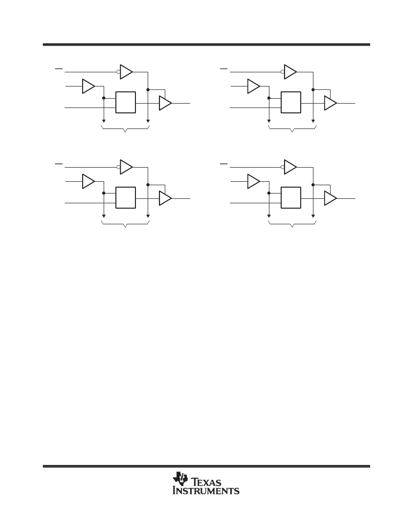
logic diagram (positive logic)
1OE
1CLK
1D1
To Seven Other Channels
1Q1
C1
1D
A3
A4
A5
A2
2OE
2CLK
2D1
To Seven Other Channels
2Q1
C1
1D
H3
H4
E5
E2
3OE
3CLK
3D1
To Seven Other Channels
3Q1
C1
1D
J3
J4
J5
J2
4OE
4CLK
4D1
To Seven Other Channels
4Q1
C1
1D
T3
T4
N5
N2
NOTE A: 1VCC is associated with these channels.
NOTE B: 2VCC is associated with these channels.
absolute maximum ratings over operating free-air temperature range (unless otherwise noted)
Supply voltage range, V
CC
Input voltage range, V
I
(see Note 1)
Voltage range applied to any output in
the high-impedance or power-off state, V
O
(see Note 1)
. . . . . . . . . . . . . . . . . . . . . . . . . . . . . . . . . . . . . . . . . . . . . . . . . . . . . . . . . . . . . . . . . . . .
Voltage range applied to any output in the high state, V
O
(see Note 1)
Output current in the low state, I
O
: SN54ALVTH32374
SN74ALVTH32374
Output current in the high state, I
O
: SN54ALVTH32374
SN74ALVTH32374
Input clamp current, I
IK
(V
I
< 0)
. . . . . . . . . . . . . . . . . . . . . . . . . . . . . . . . . . . . . . . . . . . . . . . . . . . . . . . . . . .
Output clamp current, I
OK
(V
O
< 0)
. . . . . . . . . . . . . . . . . . . . . . . . . . . . . . . . . . . . . . . . . . . . . . . . . . . . . . . .
Package thermal impedance,
θ
JA
(see Note 2)
. . . . . . . . . . . . . . . . . . . . . . . . . . . . . . . . . . . . . . . . . . . . .
Storage temperature range, T
stg
. . . . . . . . . . . . . . . . . . . . . . . . . . . . . . . . . . . . . . . . . . . . . . . . . . .
Stresses beyond those listed under “absolute maximum ratings” may cause permanent damage to the device. These are stress ratings only, and
functional operation of the device at these or any other conditions beyond those indicated under “recommended operating conditions” is not
implied. Exposure to absolute-maximum-rated conditions for extended periods may affect device reliability.
NOTES:
1. The input and output negative-voltage ratings may be exceeded if the input and output clamp-current ratings are observed.
2. The package thermal impedance is calculated in accordance with JESD 51.
–0.5 V to 4.6 V
–0.5 V to 7 V
. . . . . . . . . . . . . . . . . . . . . . . . . . . . . . . . . . . . . . . . . . . . . . . . . . . . . . . . .
. . . . . . . . . . . . . . . . . . . . . . . . . . . . . . . . . . . . . . . . . . . . . . . . . .
–0.5 V to 7 V
–0.5 V to 7 V
. . . . . . . . . . . . . . . . . . . .
96 mA
128 mA
–48 mA
–64 mA
–50 mA
–50 mA
40
°
C/W
. . . . . . . . . . . . . . . . . . . . . . . . . . . . . . . . . . . . . . . .
. . . . . . . . . . . . . . . . . . . . . . . . . . . . . . . . . . . . . . .
. . . . . . . . . . . . . . . . . . . . . . . . . . . . . . . . . . . . . .
. . . . . . . . . . . . . . . . . . . . . . . . . . . . . . . . . . . . . .
–65
°
C to 150
°
C
相關(guān)PDF資料 |
PDF描述 |
|---|---|
| SN54ALVTHR16245WD | 2.5-V/3.3-V 16-BIT BUS TRANSCEIVERS WITH 3-STATE OUTPUTS |
| SN74ALVTHR16245DGG | 2.5-V/3.3-V 16-BIT BUS TRANSCEIVERS WITH 3-STATE OUTPUTS |
| SN74ALVTHR16245DGV | 2.5-V/3.3-V 16-BIT BUS TRANSCEIVERS WITH 3-STATE OUTPUTS |
| SNJ54ALVTHR16245W | 2.5-V/3.3-V 16-BIT BUS TRANSCEIVERS WITH 3-STATE OUTPUTS |
| SN54AS1010A | Triple 3-Input Positive-Nand Buffers(三3輸入正與非緩沖器) |
相關(guān)代理商/技術(shù)參數(shù) |
參數(shù)描述 |
|---|---|
| SN54AS00J | 制造商:Texas Instruments 功能描述:QUAD 2-INPUT NAND GATE - Rail/Tube |
| SN54AS04J | 制造商:Texas Instruments 功能描述:HEX INVERTER - Rail/Tube |
| SN54AS08J | 制造商:Texas Instruments 功能描述:AND Gate 4-Element 2-IN Bipolar 14-Pin CDIP Tube 制造商:Texas Instruments 功能描述:AND GATE 4-ELEM 2-IN BIPOLAR 14CDIP - Rail/Tube |
| SN54AS08W | 制造商:Texas Instruments 功能描述: |
| SN54AS1004AJ | 制造商:Texas Instruments 功能描述:Driver 6-CH Inverting Bipolar 14-Pin CDIP Tube |
發(fā)布緊急采購,3分鐘左右您將得到回復(fù)。