- 您現(xiàn)在的位置:買賣IC網(wǎng) > PDF目錄374850 > SN54ALS996JT (Texas Instruments, Inc.) 8-BIT D-TYPE EDGE-TRIGGERED READ-BACK LATCHES PDF資料下載
參數(shù)資料
| 型號(hào): | SN54ALS996JT |
| 廠商: | Texas Instruments, Inc. |
| 元件分類: | 通用總線功能 |
| 英文描述: | 8-BIT D-TYPE EDGE-TRIGGERED READ-BACK LATCHES |
| 中文描述: | 8位D型邊沿觸發(fā)回讀鎖存 |
| 文件頁數(shù): | 1/9頁 |
| 文件大小: | 133K |
| 代理商: | SN54ALS996JT |
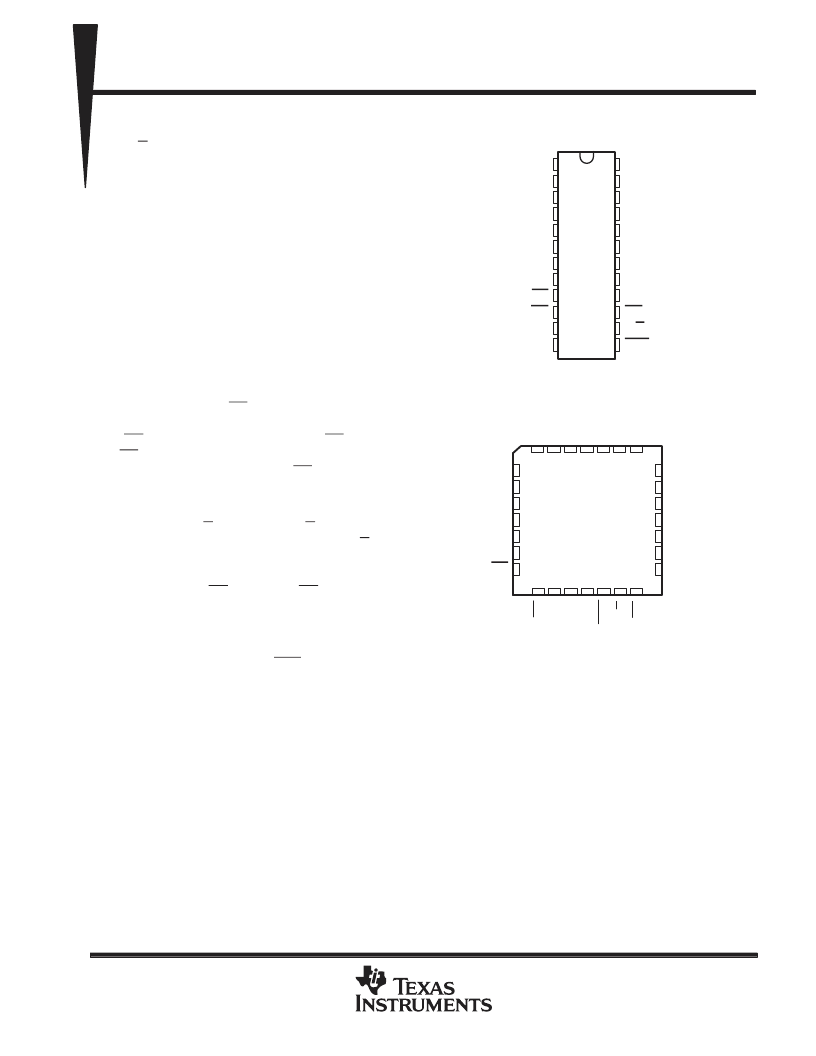
SN54ALS996 . . . JT PACKAGE
SN74ALS996 . . . DW OR NT PACKAGE
(TOP VIEW)
SN54ALS996 . . . FK PACKAGE
(TOP VIEW)
1
2
3
4
5
6
7
8
9
10
11
12
24
23
22
21
20
19
18
17
16
15
14
13
1D
2D
3D
4D
5D
6D
7D
8D
EN
RD
CLK
GND
V
CC
1Q
2Q
3Q
4Q
5Q
6Q
7Q
8Q
OE
T/C
CLR
NC – No internal connection
3 2 1 28 27
12 13
5
6
7
8
9
10
11
25
24
23
22
21
20
19
3Q
4Q
5Q
NC
6Q
7Q
8Q
4D
5D
6D
NC
7D
8D
EN
4
26
14 15 16 17 18
R
C
G
N
C
T
O
3
2
1
N
1
2
V
C
C
SN54ALS996, SN74ALS996
8-BIT D-TYPE EDGE-TRIGGERED READ-BACK LATCHES
SDAS098B – OCTOBER 1984 – REVISED JANUARY 1995
Copyright
1995, Texas Instruments Incorporated
2–1
POST OFFICE BOX 655303
DALLAS, TEXAS 75265
3-State I/O-Type Read-Back Inputs
Bus-Structured Pinout
T/C Determines True or Complementary
Data at Q Outputs
Package Options Include Plastic
Small-Outline (DW) Packages, Ceramic
Chip Carriers (FK), and Standard Plastic
(NT) and Ceramic (JT) 300-mil DIPs
description
These 8-bit latches are designed specifically for
storing the contents of the input data bus and
providing the capability of reading back the stored
data onto the input data bus. The Q outputs are
designed with bus-driving capability.
The edge-triggered flip-flops enter the data on the
low-to-high transition of the clock (CLK) input
when the enable (EN) input is low. Data can be
read back onto the data inputs by taking the read
(RD) input low, in addition to having EN low. When
EN is high, both the read-back and write modes
are disabled. Transitions on EN should only be
made with CLK high to prevent false clocking.
The polarity of the Q outputs can be controlled by
the polarity (T/C) input. When T/C is high, Q is the
same as is stored in the flip-flops. When T/C is low,
the output data is inverted. The Q outputs can be
placed in the high-impedance state by taking the
output-enable (OE) input high. OE does not affect
the internal operation of the register. Old data can
be retained or new data can be entered while the
outputs are off.
A low level at the clear (CLR) input resets the
internal registers low. The clear function is
asynchronous and overrides all other register
functions.
The -1 version of the SN74ALS996 is identical to the standard version, except that the recommended maximum
I
OL
for the -1 version is increased to 48 mA. There is no -1 version of the SN54ALS996.
The SN54ALS996 is characterized for operation over the full military temperature range of –55
°
C to 125
°
C. The
SN74ALS996 is characterized for operation from 0
°
C to 70
°
C.
PRODUCTION DATA information is current as of publication date.
Products conform to specifications per the terms of Texas Instruments
standard warranty. Production processing does not necessarily include
testing of all parameters.
相關(guān)PDF資料 |
PDF描述 |
|---|---|
| SN54ALVTH16244WD | 2.5-V/3.3-V 16-BIT BUFFERS/DRIVERS WITH 3-STATE OUTPUTS |
| SN74ALVTH16244DGV | 2.5-V/3.3-V 16-BIT BUFFERS/DRIVERS WITH 3-STATE OUTPUTS |
| SN74ALVTH16244DGG | 2.5-V/3.3-V 16-BIT BUFFERS/DRIVERS WITH 3-STATE OUTPUTS |
| SN54AS1004AFK | HEX INVERTING DRIVERS |
| SN54AS181BJW | ARITHMETIC LOGIC UNITS/FUNCTION GENERATORS |
相關(guān)代理商/技術(shù)參數(shù) |
參數(shù)描述 |
|---|---|
| SN54AS00J | 制造商:Texas Instruments 功能描述:QUAD 2-INPUT NAND GATE - Rail/Tube |
| SN54AS04J | 制造商:Texas Instruments 功能描述:HEX INVERTER - Rail/Tube |
| SN54AS08J | 制造商:Texas Instruments 功能描述:AND Gate 4-Element 2-IN Bipolar 14-Pin CDIP Tube 制造商:Texas Instruments 功能描述:AND GATE 4-ELEM 2-IN BIPOLAR 14CDIP - Rail/Tube |
| SN54AS08W | 制造商:Texas Instruments 功能描述: |
| SN54AS1004AJ | 制造商:Texas Instruments 功能描述:Driver 6-CH Inverting Bipolar 14-Pin CDIP Tube |
發(fā)布緊急采購,3分鐘左右您將得到回復(fù)。