- 您現(xiàn)在的位置:買(mǎi)賣(mài)IC網(wǎng) > PDF目錄385848 > SMA53 Cascadable Amplifier 10 to 500 MHz PDF資料下載
參數(shù)資料
| 型號(hào): | SMA53 |
| 英文描述: | Cascadable Amplifier 10 to 500 MHz |
| 中文描述: | 級(jí)聯(lián)放大器10至500 MHz |
| 文件頁(yè)數(shù): | 1/2頁(yè) |
| 文件大?。?/td> | 365K |
| 代理商: | SMA53 |
Cascadable Amplifier
10 to 500 MHz
A53/ SMA53
M/A-COM Inc. and its affiliates reserve the right to make changes to the
product(s) or information contained herein without notice. M/A-COM makes
no warranty, representation or guarantee regarding the suitability of its
products for any particular purpose, nor does M/A-COM assume any liability
whatsoever arising out of the use or application of any product(s) or
information.
North America
Tel: 800.366.2266 / Fax: 978.366.2266
Europe
Tel: 44.1908.574.200 / Fax: 44.1908.574.300
Asia/Pacific
Tel: 81.44.844.8296 / Fax: 81.44.844.8298
Visit www.macom.com
for additional data sheets and product information.
V2
1
Electrical Specifications: Z
0
= 50
, V
CC
= +15 V
DC
Parameter
Units
Typical
Guaranteed
25oC
0o to 50oC -54o to +85oC*
Frequency
MHz
5-600
10-500
10-500
Small Signal Gain (min)
dB
15.0
14.0
13.5
Gain Flatness (max)
dB
±0.5
±0.8
±1.0
Reverse Isolation
dB
20
Noise Figure (max)
dB
3.0
3.5
4.0
Power Output
@ 1 dB comp. (min)
dBm
3.5
2.0
1.5
IP3
dBm
+16
IP2
dBm
+22
Second Order Harmonic IP
dBm
+28
VSWR Input / Output (max)
1.5:1 / 1.5:1
2.0:1 / 2.0:1
2.1:1 / 2.1:1
DC Current @ 15 Volts (max)
mA
12
15
17
Features
AVAILABLE IN SURFACE MOUNT
LOW NOISE: 3.0 dB (TYP.)
MEDIUM THIRD ORDER I.P.: +16 dBm (TYP.)
MEDIUM GAIN 15 dB (TYP.)
Description
The A53 RF amplifier is a discrete hybrid design, which uses
thin film manufacturing processes for accurate performance and
high reliability.
This single stage bipolar transistor feedback amplifier design
displays impressive performance over a broadband frequency
range. Both TO-8 and Surface Mount packages are
Hermetically sealed, and MIL-STD-883 environmental screening
is available
.
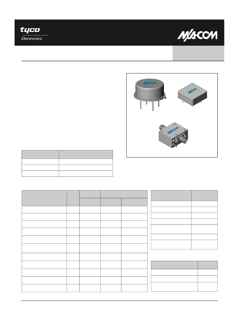
Product Image
Ordering Information
Part Number
Package
A53
TO-8
SMA53
Surface Mount
CA53
SMA Connectorized
Absolute Maximum Ratings
Parameter
Absolute
Maximum
Storage Temperature
-62oC to +125oC
Case Temperature
125oC
DC Voltage
+17 V
Continuous Input Power
+13 dBm
Short Term Input power
(1 minute max.)
50 mW
Peak Power (3 μsec max.)
0.5 W
“S” Series Burn-In
Temperature (case)
125oC
Thermal Data: V
CC
= +15 V
DC
Parameter
Rating
Thermal Resistance θ
jc
45oC/W
Transistor Power Dissipation P
d
0.111 W
Junction Temperature Rise
Above Case T
jc
5oC
* Over temperature performance limits for part number CA53, guaranteed from 0
o
C to +50
o
C only.
相關(guān)PDF資料 |
PDF描述 |
|---|---|
| SMA55 | Cascadable Amplifier 10 to 500 MHz |
| SMA611 | Cascadable Amplifier 5 to 700 MHz |
| SMA70-1 | Cascadable Amplifier 10 to 250 MHz |
| SMA75-2 | Cascadable Amplifier 5 to 250 MHz |
| SMA87-1 | 10 TO 400 MHz TO-8 CASCADABLE AMPLIFIER |
相關(guān)代理商/技術(shù)參數(shù) |
參數(shù)描述 |
|---|---|
| SMA531 | 制造商:M/A-COM Technology Solutions 功能描述:GAIN BLOCK |
| SMA54 | 制造商:MIC 制造商全稱(chēng):MIC GROUP RECTIFIERS 功能描述:SURFACE MOUNT TRANSIENT VOLTAGE SUPPRESSOR |
| SMA540B | 功能描述:兩極晶體管 - BJT NPN Hi-Gain Lo-Noise RoHS:否 制造商:STMicroelectronics 配置: 晶體管極性:PNP 集電極—基極電壓 VCBO: 集電極—發(fā)射極最大電壓 VCEO:- 40 V 發(fā)射極 - 基極電壓 VEBO:- 6 V 集電極—射極飽和電壓: 最大直流電集電極電流: 增益帶寬產(chǎn)品fT: 直流集電極/Base Gain hfe Min:100 A 最大工作溫度: 安裝風(fēng)格:SMD/SMT 封裝 / 箱體:PowerFLAT 2 x 2 |
| SMA540BTR | 制造商:STMicroelectronics 功能描述:TRANS GP BJT NPN 4.5V 0.04A 4PIN SOT-323 - Tape and Reel |
| SMA54A | 制造商:MIC 制造商全稱(chēng):MIC GROUP RECTIFIERS 功能描述:SURFACE MOUNT TRANSIENT VOLTAGE SUPPRESSOR |
發(fā)布緊急采購(gòu),3分鐘左右您將得到回復(fù)。