- 您現(xiàn)在的位置:買(mǎi)賣(mài)IC網(wǎng) > PDF目錄372133 > SDM-09120 925-960 MHz Class AB 130W Power Amplifier Module PDF資料下載
參數(shù)資料
| 型號(hào): | SDM-09120 |
| 英文描述: | 925-960 MHz Class AB 130W Power Amplifier Module |
| 中文描述: | 925-960兆赫AB類(lèi)130瓦功率放大器模塊 |
| 文件頁(yè)數(shù): | 2/5頁(yè) |
| 文件大小: | 204K |
| 代理商: | SDM-09120 |
303 S. Technology Court
Broomfield, CO 80021
Phone: (800) SMI-MMIC
2
http://www.sirenza.com
EDS-103478 Rev E
SDM-09120 925-960 MHz 130W Power Amp Module
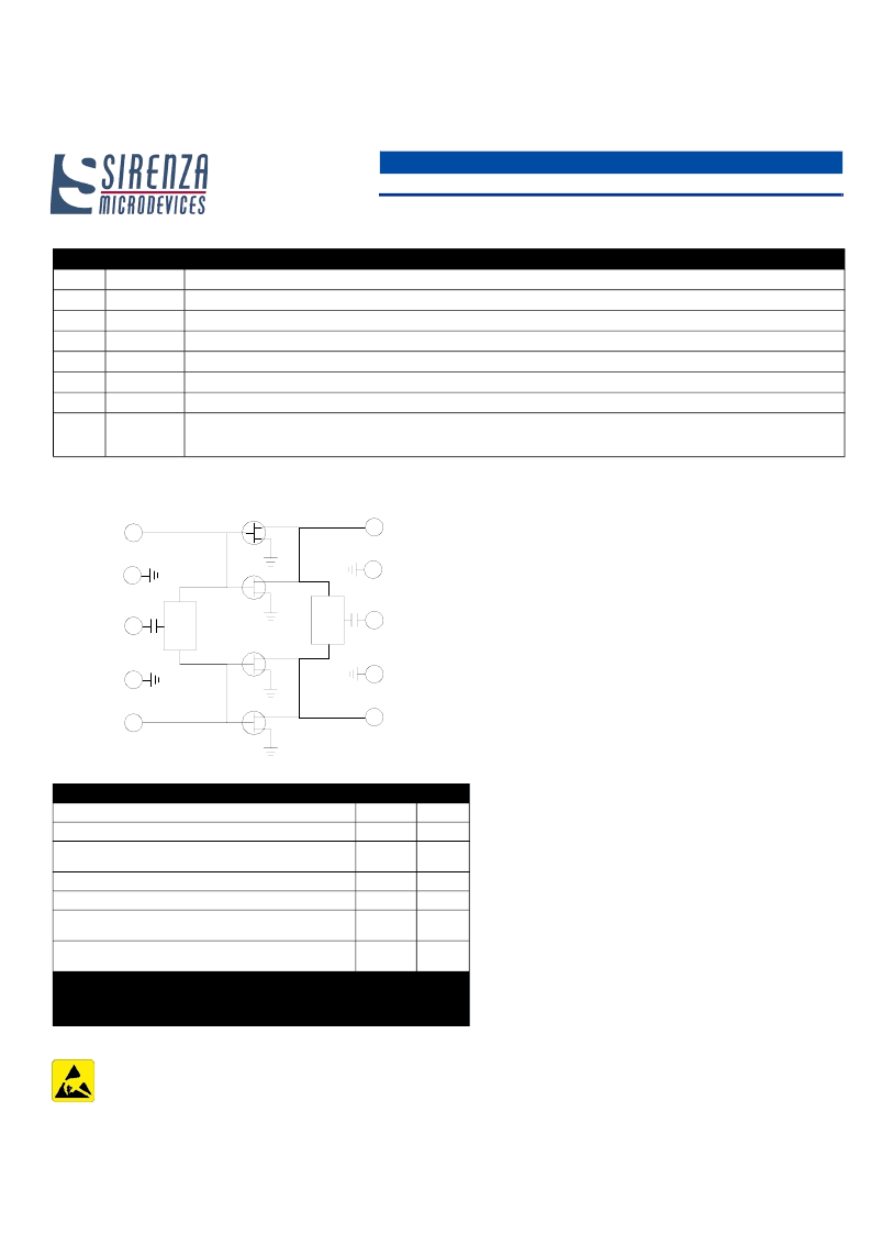
Pin Description
Pin #
Function
Description
1
V
GS1
Ground
LDMOS FET Q1 and Q2 gate bias. V
GSTH
3.0 to 5.0 VDC. See Notes 2, 3 and 4
Module Topside ground.
2,4,7,9
3
RF Input
Internally DC blocked
5
V
GS2
V
D2
LDMOS FET Q3 and Q4 gate bias. V
GSTH
3.0 to 5.0 VDC. See Notes 2, 3 and 4
LDMOS FET Q3 and Q4 drain bias. See Note 1.
6
8
RF Output
Internally DC blocked
10
V
D1
LDMOS FET Q1 and Q2 drain bias. See Note 1.
Flange
Ground
Baseplate provides electrical ground and a thermal transfer path for the device. Proper mounting assures
optimal performance and the highest reliability. See Sirenza applications note AN-054 Detailed Installation Instructions for
Power Modules.
Caution: ESD Sensitive
Appropriate precaution in handling, packaging
and testing devices must be observed.
Note 1:
Internal RF decoupling is included on all bias leads. No addi-
tional bypass elements are required, however some applica-
tions may require energy storage on the V
D
leads to
accommodate modulated signals.
Note 2:
Gate voltage must be applied to V
GS
leads simultaneously with
or after application of drain voltage to prevent potentially
destructive oscillations. Bias voltages should never be applied
to a module unless it is properly terminated on both input and
output.
Note 3:
The required V
GS
corresponding to a specific I
DQ
will vary from
module to module and may differ between V
GS1
and V
GS2
on
the same module by as much as ±0.10 volts due to the normal
die-to-die variation in threshold voltage for LDMOS transistors.
Note 4:
The threshold voltage (V
GSTH
) of LDMOS transistors varies with
device temperature. External temperature compensation may
be required. See Sirenza application notes AN-067 LDMOS
Bias Temperature Compensation.
Note 5:
This module was designed to have it's leads hand
soldered to an adjacent PCB. The maximum soldering iron tip
temperature should not exceed 700° C, and the soldering iron
tip should not be in direct contact with the lead for longer than
10 seconds. Refer to app note AN054 (www.sirenza.com) for
further installation instructions.
Absolute Maximum Ratings
Parameters
Value
Unit
Drain Voltage (V
DD
)
RF Input Power
35
V
+43
dBm
Load Impedance for Continuous Operation
Without Damage
5:1
VSWR
Control (Gate) Voltage, VDD = 0 VDC
15
V
Output Device Channel Temperature
+200
oC
Operating Temperature Range
-20 to
+90
oC
Storage Temperature Range
-40 to
+100
oC
Operation of this device beyond any one of these limits may cause per-
manent damage. For reliable continuous operation see typical setup val-
ues specified in the table on page one.
+28V DC
Q4
Q3
Q2
Q1
Balun
10
8
6
9
7
+28V DC
o
180
o
0
+3V DC to +6 V DC
0
o
180
o
+3V DC to +6 V DC
4
2
5
3
1
Balun
Simplified Device Schematic
相關(guān)PDF資料 |
PDF描述 |
|---|---|
| SDM-09120Y | 925-960 MHz Class AB 130W Power Amplifier Module |
| SDM872K | 16 Single Ended/8 Differential Input 12-BIT DATA ACQUISITION SYSTEMS |
| SDM862 | 16 Single Ended/8 Differential Input 12-BIT DATA ACQUISITION SYSTEMS |
| SDM862A | 16 Single Ended/8 Differential Input 12-BIT DATA ACQUISITION SYSTEMS |
| SDM862B | 16 Single Ended/8 Differential Input 12-BIT DATA ACQUISITION SYSTEMS |
相關(guān)代理商/技術(shù)參數(shù) |
參數(shù)描述 |
|---|---|
| SDM-09120_1 | 制造商:SIRENZA 制造商全稱(chēng):SIRENZA 功能描述:925-960 MHz Class AB 130W Power Amplifier Module |
| SDM-09120-1Y | 制造商:SIRENZA 制造商全稱(chēng):SIRENZA 功能描述:915-960 MHz Class AB 130W Power Amplifier |
| SDM-09120Y | 制造商:SIRENZA 制造商全稱(chēng):SIRENZA 功能描述:925-960 MHz Class AB 130W Power Amplifier Module |
| SDM-09-A-SG-0 | 功能描述:記憶卡連接器 Secure Digital Metal Cover Type RoHS:否 制造商:Yamaichi Electronics 產(chǎn)品:Card Connectors 卡類(lèi)型:microSD 類(lèi)型: 節(jié)距: 方向: 安裝風(fēng)格:SMD/SMT 端接類(lèi)型: 排數(shù): 觸點(diǎn)數(shù)量: 電流額定值:0.5 A 電壓額定值:50 V |
| SDM100 | 制造商:未知廠家 制造商全稱(chēng):未知廠家 功能描述:Logic IC |
發(fā)布緊急采購(gòu),3分鐘左右您將得到回復(fù)。