- 您現(xiàn)在的位置:買賣IC網(wǎng) > PDF目錄374734 > SC613IMLTRT (Semtech Corporation) Low Noise Regulated Charge Pump with Selectable Output PDF資料下載
參數(shù)資料
| 型號: | SC613IMLTRT |
| 廠商: | Semtech Corporation |
| 英文描述: | Low Noise Regulated Charge Pump with Selectable Output |
| 中文描述: | 低噪聲電荷泵輸出的可選 |
| 文件頁數(shù): | 5/14頁 |
| 文件大小: | 386K |
| 代理商: | SC613IMLTRT |
5
2005 Semtech Corp.
www.semtech.com
SC613
POWER MANAGEMENT
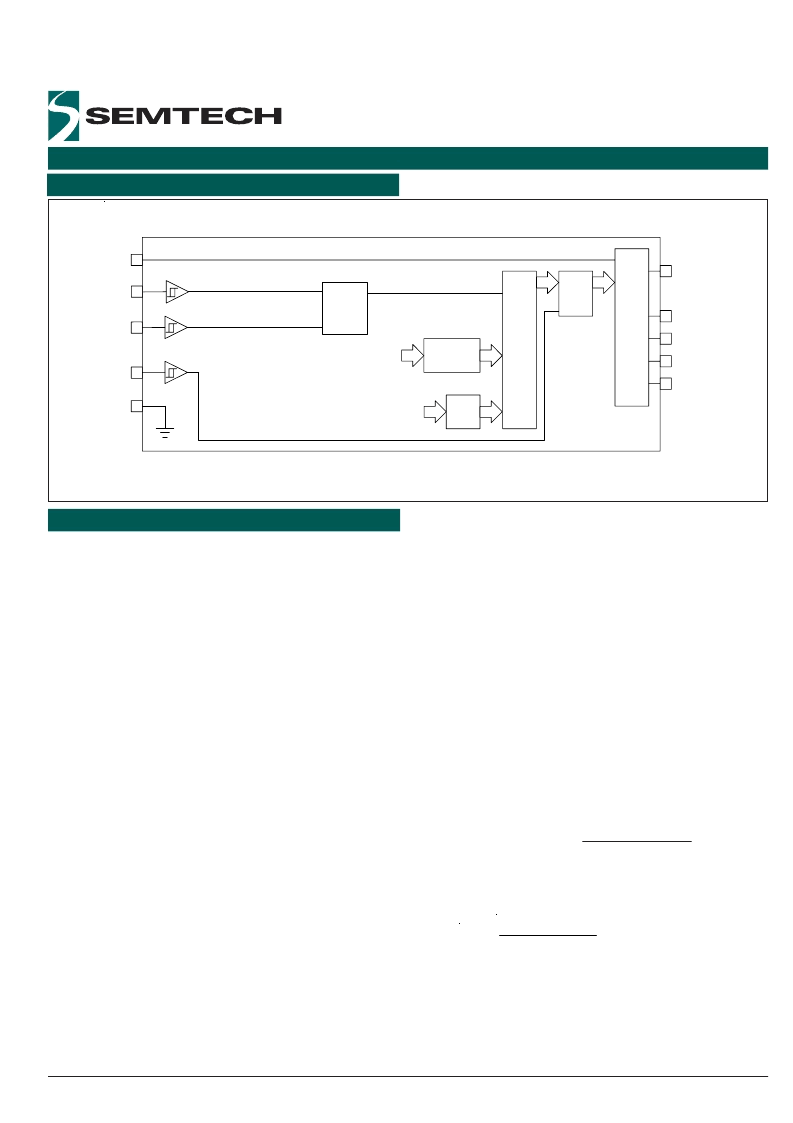
Block Diagram
Applications Information
Charge Pump Doubler Type
The SC613 uses a voltage doubler circuit which is implemented
with two switched or ‘bucket’ capactors. Most charge pump dou-
blers use only one bucket capacitor. Two bucket capacitors switch-
ing on alternate phases greatly reduce the output ripple voltage
and also reduce the size requirement for the output capacitor.
Over Voltage Protection
The output is prevented from exceeding 6.0V. This feature allows
the use of 6.3V ceramic capacitors.
Comparison with Other Regulation Methods
In many instances, a charge pump regulator is the best choice for
portable power applications. These regulators offer many advan-
tages over switch mode regulators. A smaller bill of materials,
less layout area, lower component height, less noise, no EMF, and
less overall circuit cost are typical reasons to use this type of
regulation. The efficiency of a charge pump regulator often ap-
proaches and in some cases exceeds the efficiency of a switch
mode regulator.
Inductors are often the largest and most expensive discrete com-
ponent in a design. There are no inductors used in the SC613, so
the inductor’s cost and layout area are eliminated. The noise and
EMF associated with the inductor are also eliminated.
The SC613’s fixed frequency harmonics are an advantage in por-
table communications equipment, such as cellular telephones.
The SC613 has distinct frequencies of operation, so the harmon-
ics are predictable. The harmonics are not fixed in a switch mode
regulator. Switch mode regulators have harmonics which vary
due to the pulse width modulation used to regulate the output.
Varying harmonics can be a problem because it may be more
EN
FSEL
VSEL
GND
VIN
6
5
4
4
5
8
3
MODE
SELECT
DRIVERS
SWITCH
BLOCK
TIMER
COMPARATORS
VIN
VOUT
VREF
VIN
CF1+
CF1-
CF2+
CF2-
VOUT
2
9
10
7
1
EN
OSC
650kHz or 262kHz
5.0V or 4.5V
difficult to ensure acceptable noise performance over the entire
operating range.
Many switch mode regulators have increased voltage ripple on
the output during pulse skipping mode due to the fact that there
are large periods of time when no current is supplied to the output.
The SC613 supplies current to the output continuously, so the
voltage ripple is less than a switch mode regulator, even with greatly
reduced output capacitance.
Frequency Selection
The FSEL input is for frequency selection. A logic High level at this
input will set the clock frequency to 650kHz, while a logic Low sets
the clock to 262kHz. Input from a uP or other device may be used
to change the charge pump frequency at any time. The optimal
frequency will depend upon the capacitor values, the load current,
and the exceptable amount of output ripple.
Ripple Performance
Examples of the output ripple per charge pump frequency and
output voltage are listed in the Ripple Performance table on page
5.
Efficiency
Efficiency for the SC613 is defined as,
=
η
where
V
O
= output voltage
I
O
= output current
V
IN
= input voltage
I
= quiescent current [from Electrical Characteristics
on page 2].
V
O
I
O
(
V
IN
2 I
O
I
Q
+
)
相關(guān)PDF資料 |
PDF描述 |
|---|---|
| SC614-RL1 | Speech And Music Processor |
| SC-614 | Speech And Music Processor |
| SC614-R | Speech And Music Processor |
| SC614 | Low Noise Backlight and Flash Driver With Serial Interface |
| SC614DB | Low Noise Backlight and Flash Driver With Serial Interface |
相關(guān)代理商/技術(shù)參數(shù) |
參數(shù)描述 |
|---|---|
| SC614 | 制造商:SEMTECH 制造商全稱:Semtech Corporation 功能描述:Low Noise Backlight and Flash Driver With Serial Interface |
| SC-614 | 制造商:未知廠家 制造商全稱:未知廠家 功能描述:Speech And Music Processor |
| SC61-40 | 制造商:Teledyne Relays 功能描述:RLY SSR 50MA 1.5V DC-IN 0.4A 400V DC-OUT 6PDIP SMD - Rail/Tube 制造商:Teledyne MIL SSR 功能描述:Relay SSR 50mA 1.5V DC-IN 0.4A 400V DC-OUT 6-Pin PDIP SMD |
| SC614DB | 制造商:SEMTECH 制造商全稱:Semtech Corporation 功能描述:Low Noise Backlight and Flash Driver With Serial Interface |
| SC614EVB | 制造商:SEMTECH 制造商全稱:Semtech Corporation 功能描述:Low Noise Backlight and Flash Driver With Serial Interface |
發(fā)布緊急采購,3分鐘左右您將得到回復。