- 您現(xiàn)在的位置:買(mǎi)賣IC網(wǎng) > PDF目錄374714 > SC1403ITSTRT (Semtech Corporation) Mobile Multi-Output PWM Controller with Lossless Current Sense PDF資料下載
參數(shù)資料
| 型號(hào): | SC1403ITSTRT |
| 廠商: | Semtech Corporation |
| 英文描述: | Mobile Multi-Output PWM Controller with Lossless Current Sense |
| 中文描述: | 移動(dòng)多輸出PWM控制器與無(wú)損電流檢測(cè) |
| 文件頁(yè)數(shù): | 22/31頁(yè) |
| 文件大?。?/td> | 576K |
| 代理商: | SC1403ITSTRT |
第1頁(yè)第2頁(yè)第3頁(yè)第4頁(yè)第5頁(yè)第6頁(yè)第7頁(yè)第8頁(yè)第9頁(yè)第10頁(yè)第11頁(yè)第12頁(yè)第13頁(yè)第14頁(yè)第15頁(yè)第16頁(yè)第17頁(yè)第18頁(yè)第19頁(yè)第20頁(yè)第21頁(yè)當(dāng)前第22頁(yè)第23頁(yè)第24頁(yè)第25頁(yè)第26頁(yè)第27頁(yè)第28頁(yè)第29頁(yè)第30頁(yè)第31頁(yè)
22
2004 Semtech Corp.
SC1403
PRELIMINARY
POWER MANAGEMENT
Applications Information (Cont.)
United States Patent No. 6,377,032
www.semtech.com
Operation Below 6V input
The SC1403 will operate below 6V input voltage with careful
design, but there are limitations. The first limitation is the
maximum available duty cycle from the SC1403, which limits the
obtainable output voltage. The design should minimize all circuit
losses through the system in order to deliver maximum power to
the output.
A second limitation with operation below 6V is transient response.
When load current increases rapidly, the output voltage drops
slightly; the feedback loop normally increases duty cycle briefly to
bring the output voltage back up. If duty cycle is already near the
maximum limit, the duty cycle cannot increase enough to meet
the demand, and the output voltage sags more than normal. This
problem can not be solved by changing the feedback
compensation, it is a function of the input voltage, duty cycle, and
inductor and capacitor values.
If an application requires 5V output from an input voltage below
6V, the following guidelines should be used:
1 - Set the switching frequency to 200 kHz (Tie SYNC to
GND). This increases the maximum duty cycle
compared to 300 kHz operation.
2 - Minimize the resistance in the power train. Select
mosfets, inductor, and current sense resistor to provide
the lowest resistance as is practical.
3 - Minimize the pcb resistance for all traces carrying
high current. This includes traces to the input
capacitors, mosfets and diodes, inductor, current sense
resistor, and output capacitor.
4 - Minimize the resistance between the SC1403
circuit and the power source (battery, battery charger,
AC adaptor).
5 - Use low ESR capacitors on the input to prevent the
input voltage dropping during on-time.
6 - If large load transients are expected, high
capacitance and low ESR capacitors should be used on
both the input and output.
Overvoltage Test
Measuring the overvoltage trip point can be problematic. Any
buck converter with synchronous mosfets can act as a boost con-
verter, sending energy from output to input. In some cases the
energy sent to the input is enough to drive the input voltage be-
yond normal levels, causing input overvoltage. To prevent this
enable the SC1403 PSAVE# feature, which effectively disables
the low side mosfet drive so that little energy, if any, is transferred
back to the input.
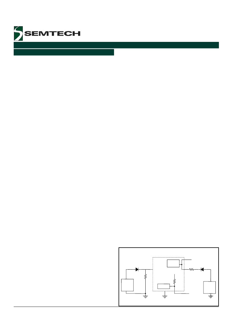
Semtech recommends the following circuit for measuring the ov-
ervoltage trip point. D1 prevents the output voltage from damag-
ing lab supply 1. R1 limits the amount of energy that can be cycled
from the output to the input. R2 absorbs the energy that might
flow from output to input, and D2 protects lab supply from pos-
sible damage. The ON5 signal is monitored to indicate when
overvoltage occurs.
Initial conditions:
Both lab supplies set to zero volts
No load connected to 3V or 5V
PSAVE# enabled (PSAVE# tied to GND)
ON5, ON3 both enabled
DVMs monitoring ON5 and the output under test
Oscilloscope probe connected to Phase Node
of the output under test (not strictly required)
Set lab supply 2 to provide 10V at the SC1403 input. The phase
node of the output being tested should show some switching ac-
tivity. The ON5 pin should be above 4V.
Slowly increase lab supply 1 until the output under test rises
slightly above it’s normal DC level. As the input lab supply 1 in-
creases, switching activity at the phase node will cease. The ON5
pin should remain above 4V.
Increase lab supply 1 in very small increments, monitoring both
ON5 and the output under test. The overvoltage trip point is the
highest voltage seen at the output before ON5 pulls low (approxi-
mately 0.3V). Do not record the voltage seen at the output after
ON5 has pulled low; when ON5 pulls low, the current flowing in D1
changes, corrupting the voltage seen at the output.
1K
D1
e.g. 1N4004
R2
470
1/2W
75
1/2W
to DVM
D1
e.g. 1N4004
Vin
Evaluation
Board
Supply
2
R1
Lab
Supply
Output
test
under
1
Lab
to DVM
ON5
VL
SC1403
D2
相關(guān)PDF資料 |
PDF描述 |
|---|---|
| SC1403 | Mobile Multi-Output PWM Controller with Virtual Current SenseTM |
| SC1403ITSTR | Mobile Multi-Output PWM Controller with Virtual Current SenseTM |
| SC1404_05 | Differential Input, Dual, Simultaneous Sampling, 4.25 MSPS, 14-Bit, SAR ADC, 16-TSSOP, Ind Temp |
| SC1404 | Mobile Multi-Output PWM Controller with Virtual Current Sense |
| SC1404ISSTR | Mobile Multi-Output PWM Controller with Virtual Current Sense |
相關(guān)代理商/技術(shù)參數(shù) |
參數(shù)描述 |
|---|---|
| SC1404 | 制造商:SEMTECH 制造商全稱:Semtech Corporation 功能描述:移動(dòng)多輸出PWM控制器用虛擬當(dāng)前SenseTM |
| SC1404_05 | 制造商:SEMTECH 制造商全稱:Semtech Corporation 功能描述:Mobile Multi-Output PWM Controller with Virtual Current SenseTM |
| SC1404ISSTR | 制造商:SEMTECH 制造商全稱:Semtech Corporation 功能描述:Mobile Multi-Output PWM Controller with Virtual Current SenseTM |
| SC1404ITSTR | 制造商:SEMTECH 制造商全稱:Semtech Corporation 功能描述:Mobile Multi-Output PWM Controller with Virtual Current SenseTM |
| SC1405 | 制造商:SEMTECH 制造商全稱:Semtech Corporation 功能描述:HIGH SPEED SYNCHRONOUS POWER MOSFET SMART DRIVER |
發(fā)布緊急采購(gòu),3分鐘左右您將得到回復(fù)。