- 您現(xiàn)在的位置:買賣IC網(wǎng) > PDF目錄374691 > SAF-C515-LM (SIEMENS A G) 8-Bit CMOS Microcontroller PDF資料下載
參數(shù)資料
| 型號: | SAF-C515-LM |
| 廠商: | SIEMENS A G |
| 元件分類: | 微控制器/微處理器 |
| 英文描述: | 8-Bit CMOS Microcontroller |
| 中文描述: | 8-BIT, 16 MHz, MICROCONTROLLER, PQFP80 |
| 文件頁數(shù): | 44/55頁 |
| 文件大小: | 268K |
| 代理商: | SAF-C515-LM |
第1頁第2頁第3頁第4頁第5頁第6頁第7頁第8頁第9頁第10頁第11頁第12頁第13頁第14頁第15頁第16頁第17頁第18頁第19頁第20頁第21頁第22頁第23頁第24頁第25頁第26頁第27頁第28頁第29頁第30頁第31頁第32頁第33頁第34頁第35頁第36頁第37頁第38頁第39頁第40頁第41頁第42頁第43頁當(dāng)前第44頁第45頁第46頁第47頁第48頁第49頁第50頁第51頁第52頁第53頁第54頁第55頁
C515
Semiconductor Group
44
1997-08-01
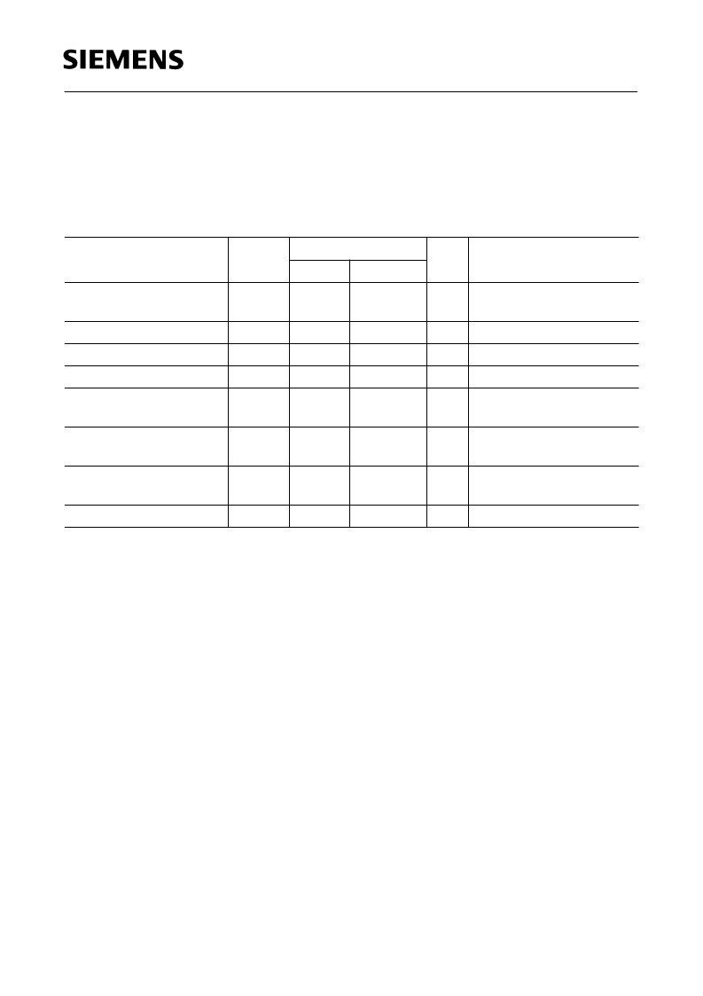
A/D Converter Characteristics
V
CC
= 5 V
+
10%, – 15%;
V
SS
= 0
V
T
A
= 0 to 70
°
C
T
A
= – 40 to 85
°
C
T
A
= – 40 to 110
°
C
for the SAB-C515-1RM
for the SAF-C515-1RM
for the SAH-C515-1RM
V
CC
– 0.25 V
≤
V
AREF
≤
V
CC
+
0.25
V
;
V
SS
– 0.2 V
≤
V
AGND
≤
V
ss
+ 0.2 V;
V
IntAREF
V
IntAGND
≥
1 V;
Notes:
1) V
AIN
may exceed V
AGND
or V
AREF
up to the absolute maximum ratings. However, the conversion result in
these cases will be 00
H
or FF
H
, respectively.
2) During the sample time the input capacitance
C
AIN
can be charged/discharged by the external source. The
internal resistance of the analog source must allow the capacitance to reach their final voltage level within t
S
.
After the end of the sample time t
S
, changes of the analog input voltage have no effect on the conversion
result.
3) This parameter includes the sample time t
S
and the conversion time t
C
. The values for the conversion clock
t
ADC
is always 8 x t
IN
.
4) T
UE
is tested at V
AREF
= 5.0 V, V
AGND
= 0 V, V
CC
= 4.9 V. It is guaranteed by design characterization for all
other voltages within the defined voltage range.
If an overload condition occurs on maximum 2 not selected analog input pins and the absolute sum of input
overload currents on all analog input pins does not exceed 10 mA, an additional conversion error of 1/2 LSB
is permissible.
5) During the conversion the ADC’s capacitance must be repeatedly charged or discharged. The internal
resistance of the reference source must allow the capacitance to reach their final voltage level within the
indicated time. The maximum internal resistance results from the programmed conversion timing.
6) Not 100% tested, but guaranteed by design characterization.
Parameter
Symbol
Limit Values
Unit
Test Condition
min.
V
AGND
-
0.2
max.
V
AREF
+
0.2
2 x
t
CLCL
16 x
t
IN
80 x
t
IN
±
1
Analog input voltage
V
AIN
V
1)
A/D converter input clock
t
IN
t
S
t
ADCC
T
UE
–
ns
Sample time
–
ns
2)
Conversion cycle time
–
ns
3)
Total unadjusted error
–
LSB
V
IntAREF
=
V
AREF
= V
CC
V
IntAGND
=
V
AGND
= V
SS
4)
t
IN
in [ns]
5) 6)
Internal resistance of
reference voltage source
R
AREF
–
8 x
t
IN
/500
- 1
t
S
/ 500 - 1
k
Internal resistance of
analog source
R
ASRC
–
k
t
S
in [ns]
2) 6)
ADC input capacitance
C
AIN
–
45
pF
6)
相關(guān)PDF資料 |
PDF描述 |
|---|---|
| SAF-C515A-LM | 8-Bit CMOS Microcontroller |
| SAF-C515C-LM | 8-Bit CMOS Microcontroller |
| SAB-C515-1R24M | 8-Bit CMOS Microcontroller |
| SAB-C515-1RM | 8-Bit CMOS Microcontroller |
| SAB-C515-L24M | 8-Bit CMOS Microcontroller |
相關(guān)代理商/技術(shù)參數(shù) |
參數(shù)描述 |
|---|---|
| SAFC515LN | 制造商:Infineon Technologies AG 功能描述:MCU 8-bit C500 8051 CISC ROMLess 5V 68-Pin PLCC |
| SAF-C515-LN | 制造商:Rochester Electronics LLC 功能描述: |
| SAF-C517A | 制造商:INFINEON 制造商全稱:Infineon Technologies AG 功能描述:8-bit CMOS MICROCONTROLLER |
| SAF-C517A-4R24M | 制造商:INFINEON 制造商全稱:Infineon Technologies AG 功能描述:8-Bit CMOS Microcontroller |
| SAF-C517A-4RM | 制造商:INFINEON 制造商全稱:Infineon Technologies AG 功能描述:8-Bit CMOS Microcontroller |
發(fā)布緊急采購,3分鐘左右您將得到回復(fù)。