- 您現(xiàn)在的位置:買賣IC網(wǎng) > PDF目錄374694 > SAE81C90 (INFINEON TECHNOLOGIES AG) Standalone Full-CAN Controller PDF資料下載
參數(shù)資料
| 型號(hào): | SAE81C90 |
| 廠商: | INFINEON TECHNOLOGIES AG |
| 英文描述: | Standalone Full-CAN Controller |
| 中文描述: | 獨(dú)立全CAN控制器 |
| 文件頁(yè)數(shù): | 37/41頁(yè) |
| 文件大小: | 521K |
| 代理商: | SAE81C90 |
第1頁(yè)第2頁(yè)第3頁(yè)第4頁(yè)第5頁(yè)第6頁(yè)第7頁(yè)第8頁(yè)第9頁(yè)第10頁(yè)第11頁(yè)第12頁(yè)第13頁(yè)第14頁(yè)第15頁(yè)第16頁(yè)第17頁(yè)第18頁(yè)第19頁(yè)第20頁(yè)第21頁(yè)第22頁(yè)第23頁(yè)第24頁(yè)第25頁(yè)第26頁(yè)第27頁(yè)第28頁(yè)第29頁(yè)第30頁(yè)第31頁(yè)第32頁(yè)第33頁(yè)第34頁(yè)第35頁(yè)第36頁(yè)當(dāng)前第37頁(yè)第38頁(yè)第39頁(yè)第40頁(yè)第41頁(yè)
07Feb95@09:05h Intermediate Version
Semiconductor Group
36
SAE 81C90/91
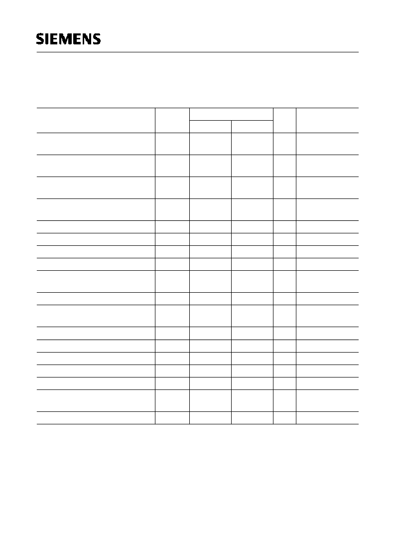
DC Characteristics
V
CC
= 5 V
±
10 %;
T
A
= – 40 to + 110 C
V
SS
= 0 V
Notes
1)
If the bus lines work according to the ISO specification, additional circuitry is necessary for interconnection of
the input comparator to the bus lines.
2)
Not 100% tested, guaranteed by design characterization.
3)
This value is a typical value!
4)
This specification does not apply to the port pins (P00...P07, P10...P17) due to the implemented pullups!
5)
In oscillator mode the size of the low-end capacitance must correspond to the specification of the crystal
manufacturer. The optimum values depend on the selected crystal, the intended frequency and the actual
application hardware (stray capacitances). 10 pF are recommended for C
L
.
For best results keep the crystal circuitry connections as short as possible and keep the CLKOUT line away
from it. If the CLKOUT signal is not required by the system it should be switched off.
Parameter
Symbol
Limit Values
Unit
Test Condition
min.
max.
0.3
V
CC
Input low voltage
(all except XTAL1 and XTAL2)
V
IL
SR 0
V
–
Input low voltage
(XTAL1 and XTAL2)
V
ILX
SR 0
0.5
V
–
Input high voltage
(all except XTAL1 and XTAL2)
V
IH
SR 0.7
V
CC
V
CC
V
–
Input high voltage
(XTAL1 and XTAL2)
Comparator input voltage
1)
Common mode voltage
2)
Hysteresis
2)
Offset voltage
2)
V
IHX
SR
V
CC
– 1.0
V
CC
V
–
V
CI
V
ICOM
SR 1.5
V
HYS
DC –
V
OFF
DC –
V
OL
DC –
SR 0.5
V
CC
+ 0.5
V
CC
– 1.5
100
3)
100
3)
0.2
V
CC
V
–
V
–
mV
–
mV
–
I
OL
= 1.6 mA
Output low voltage
(all except CLKOUT, TX0, TX1)
V
Output low voltage (CLKOUT)
V
OLC
DC –
V
OH
DC 0.8
V
CC
0.4
V
CC
V
I
OL1
= 10 mA
I
OH
= – 1.6 mA
Output high voltage
(all except CLKOUT, TX0, TX1)
V
Output high voltage (CLKOUT)
V
OHC
DC
V
CC
– 0.8
I
I
DC –
I
SRC
DC 5
I
SNK
DC 5
C
L
DC 6.8
C
I
DC –
V
CC
±
1
–
V
μ
A
mA
I
OH
= – 10 mA
0 V <
V
IN
<
V
CC
4)
V
O
=
V
CC
– 1 V
V
O
= 1 V
Input leakage current
Source output current (TX0, TX1)
Sink output current (TX0, TX1)
Low end capacitance
5)
Pin capacitance
2)
–
mA
12
pF
10
pF
f
= 1 MHz
T
A
= 25 C
Power supply current
I
CC
–
30
mA
相關(guān)PDF資料 |
PDF描述 |
|---|---|
| SAE81C91 | Standalone Full-CAN Controller |
| SAE81C90-N | IC-SM-CAN CONTROLLER |
| SAF-C161K-L25M | CONNECTOR ACCESSORY |
| SAB-C161K-L25M | CONNECTOR ACCESSORY |
| SAF-C161K-LM | CONNECTOR ACCESSORY |
相關(guān)代理商/技術(shù)參數(shù) |
參數(shù)描述 |
|---|---|
| SAE81C90-N | 制造商:INFINEON 制造商全稱:Infineon Technologies AG 功能描述:IC-SM-CAN CONTROLLER |
| SAE81C91 | 制造商:SIEM 功能描述: |
| SAE92-0608 | 制造商:FW Bell 功能描述:Standard, Aluminum Stem |
| SAEAMS2404 | 制造商:ITT 制造商全稱:ITT Industries 功能描述:CONNECTORS, ELECTRIC, RECTANGULAR, NONENVIRONMENTAL, MINIATURE, POLARIZED SHELL, RACK AND PANEL, GENERAL SPECIFCATION FOR |
| SAEAMS2700 | 制造商:ITT 制造商全稱:ITT Industries 功能描述:CONNECTORS, ELECTRIC, RECTANGULAR, NONENVIRONMENTAL, MINIATURE, POLARIZED SHELL, RACK AND PANEL, GENERAL SPECIFCATION FOR |
發(fā)布緊急采購(gòu),3分鐘左右您將得到回復(fù)。